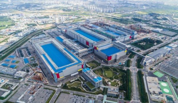
Samsung Electronics has secured an order from a Japanese artificial intelligence (AI) company to produce 2-nanometer (nm, one billionth of a meter) semiconductors using the cutting-edge semiconductor manufacturing process.
According to industry sources on the 15th, Samsung Electronics is reported to have received an order from the Japanese AI startup Preferred Networks (PFN) for AI semiconductors based on the 2-nanometer process, including AI accelerators.
Founded in 2014, PFN is recognized for its expertise in AI deep learning development and has attracted large-scale investments from major companies across various industries such as Toyota, NTT, and Fanuc.
Inside and outside the industry, it is speculated that Samsung Electronics was chosen by PFN because it possesses both memory and foundry businesses, enabling turnkey production?from design of high-bandwidth memory (HBM) to manufacturing and advanced 2.5D packaging.
Earlier, in June last year, Samsung Electronics announced a detailed roadmap for the 2-nanometer process, igniting competition in the advanced fine process field with Taiwan’s TSMC, the world’s number one foundry company. According to foreign media, TSMC has shared the results of its 2-nanometer prototype process tests with major clients such as Apple and Nvidia, and aims to start mass production in 2025, leading the 2-nanometer race.
However, Samsung Electronics has set a goal to gain a technological edge in the 2-nanometer competition based on its accumulated technology, including being the first in the world to start the 3-nanometer process applying the next-generation transistor GAA (Gate-All-Around) in June 2022.
Kyung Kye-hyun, President of Samsung Electronics’ Device Solutions (DS) Division, said in a lecture at the Korea Advanced Institute of Science and Technology (KAIST) in Daejeon last May, "From the 2-nanometer process, even the industry leader will adopt GAA," adding, "We will catch up to the industry leader in technology within five years."
© The Asia Business Daily(www.asiae.co.kr). All rights reserved.


