Job Opportunities at Samsung Electronics in 5 Years
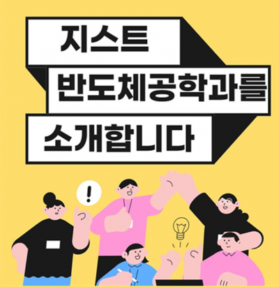
The Gwangju Institute of Science and Technology (GIST, President Lim Ki-chul) announced that it has selected the first 30 freshmen for the Department of Semiconductor Engineering (Department Head Lee Dong-seon), which aims to nurture semiconductor specialists linked to Samsung Electronics recruitment, and will start operating from March.
Starting from this year’s admission, the GIST Department of Semiconductor Engineering will select a total of 150 students through an integrated bachelor's and master's program by admitting 30 students annually until 2028. It is expected to create synergy with Samsung Electronics' global technological capabilities through the cultivation of highly skilled professionals with practical field competencies and semiconductor research and development desired by the industry.
GIST and Samsung Electronics signed a memorandum of understanding last March to establish a contract department for training specialized semiconductor process technicians, agreeing to operate a five-year integrated bachelor's and master's program linked to Samsung Electronics recruitment.
During the bachelor's program (7 semesters) and master's program (3 semesters), admitted students will receive full tuition and dormitory fees, overseas training, on-site corporate/research institute experiential learning, meetings with Samsung Electronics employees as mentors, and various benefits and opportunities to grow as experts in the semiconductor field.
After completing the regular curriculum and passing a designated exam, students can be hired by Samsung Electronics to perform semiconductor process technology and circuit design duties.
The GIST Department of Semiconductor Engineering not only possesses the Compound Semiconductor Optical Convergence Nano Process Center equipped with a total of 44 devices capable of thin film, lithography, etching, oxidation, post-processes, and physical/chemical analysis, but is also currently establishing an advanced process fab for next-generation AI semiconductor development such as chiplet heterogeneous integration and fan-out packaging.
Department Head Lee Dong-seon stated, “We are preparing a program that aims to nurture world-class industry-oriented semiconductor experts by providing education on semiconductor design and processes as well as conducting research related to the semiconductor industry field,” adding, “We will do our best to help students grow into the world’s top experts in semiconductor process fields through the GIST semiconductor specialized curriculum.”
© The Asia Business Daily(www.asiae.co.kr). All rights reserved.
![Clutching a Stolen Dior Bag, Saying "I Hate Being Poor but Real"... The Grotesque Con of a "Human Knockoff" [Slate]](https://cwcontent.asiae.co.kr/asiaresize/183/2026021902243444107_1771435474.jpg)


