BCNC Accelerates Domestic Production of Poly Silicon
Improves Self-Sufficiency in Semiconductor Etching Process Materials
Domestic Semiconductor SoBuJang Startups Also Active
A domestic materials company that has localized polycrystalline silicon (poly-Si) material used in parts for semiconductor etching processes (the process of etching only the necessary circuit patterns on semiconductor wafers) will begin mass production from the second quarter of this year. Poly-Si, along with quartz and silicon carbide, is considered a key material used in semiconductor etching processes, but the domestic poly-Si material ratio is only about 10%. This is expected to help increase the localization rate of major semiconductor materials.
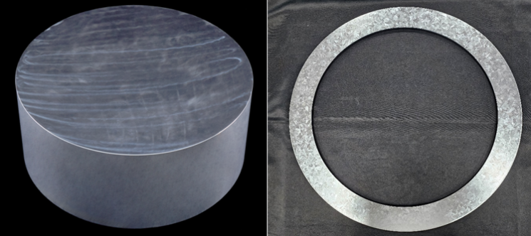 Polysilicon material used in semiconductor etching processes (left) and the focus ring component made based on this material /
 [Photo by BCN C]
According to the semiconductor industry on the 30th, BCN&C, a semiconductor materials and parts company, plans to complete the production facility for poly-Si materials used in the etching process by March and start full-scale operation. This will enable the company to supply poly-Si materials and etching rings and other parts made from them domestically in earnest.
Kim Donhan, CEO of BCN&C, said, "We have localized natural quartz material, which was previously dependent on imports, into synthetic quartz (QD9+), developed another material (CD9) to replace silicon carbide (CVD-SiC), and now we have started mass production of silicon material. We have become the world's first company to vertically integrate the key materials used in semiconductor etching processes," emphasizing the significance.
Poly-Si is ‘high-purity polycrystalline silicon’ and is a key material used in semiconductor etching processes. Although the global poly-Si market is expected to grow to about 2.5 trillion KRW this year, localization is difficult, so the domestic utilization rate remains low at 10%.
Recently, the semiconductor materials, parts, and equipment (SoBuJang) industry has been accelerating localization efforts. Hanmi Semiconductor, an equipment company, has developed and is supplying bonding equipment (TC bonder) used in producing high-bandwidth memory (HBM), which is gaining attention as AI memory semiconductors. Bonding equipment is used to attach chips.
SoBuJang startups founded by former Samsung Electronics and SK Hynix employees are also emerging one after another. Notable examples include RC Tech (equipment modification) and Oldowan (materials development), which were established through SK Hynix’s in-house venture system and are growing their businesses.
© The Asia Business Daily(www.asiae.co.kr). All rights reserved.
!["The Woman Who Threw Herself into the Water Clutching a Stolen Dior Bag"...A Grotesque Success Story That Shakes the Korean Psyche [Slate]](https://cwcontent.asiae.co.kr/asiaresize/183/2026021902243444107_1771435474.jpg)


