Where Will Samsung's 500 Trillion and SK's 122 Trillion Complex Investments Be Used?
Samsung to Start Fab 1 Construction in 2028
Hynix's First Factory in Yongin Memory Cluster to Complete in 2027
Samsung Electronics and SK Hynix plan to invest a total of 622 trillion KRW to create the world's largest and best 'semiconductor mega cluster' by 2047. This investment will be used to build non-memory (system) and memory semiconductor facilities, as well as next-generation research and development (R&D) related facilities in semiconductor sites located in Yongin, Pyeongtaek, Giheung, Gyeonggi Province.
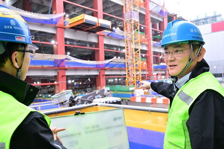 Samsung Electronics Chairman Lee Jae-yong is seen inspecting the construction site of the next-generation semiconductor R&D complex during his visit to Samsung Electronics Giheung Campus in Gyeonggi Province on October 19 last year.
 [Photo by Yonhap News]
According to the government and industry on the 15th, Samsung Electronics will invest 500 trillion KRW out of the 622 trillion KRW in Yongin, Pyeongtaek, and Giheung. First, 360 trillion KRW will be invested in the Namsa National Industrial Complex in Yongin to build six fabs (factories) and establish an 'advanced system semiconductor cluster.' The site will be prepared in 2026, and construction of Fab 1 will begin in 2028. This facility aims to start operations by 2030. Fab 1 is expected to be used as Samsung Foundry's ultra-fine process production base. Currently, Samsung Electronics is competing with the world's largest foundries such as Taiwan's TSMC and the U.S.'s Intel in foundry processes below 2 nanometers (nm; 1 nm = one billionth of a meter).
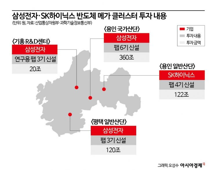
In the Pyeongtaek general industrial complex, 120 trillion KRW will be invested to establish three new fabs. Here, research will be conducted on next-generation devices such as ferroelectrics and magnetic materials, as well as advanced packaging technologies like vertical stacking and heterogeneous integration to improve the efficiency of AI semiconductor HBM (High Bandwidth Memory). Industry-academia cooperation with the newly established KAIST Pyeongtaek campus will also be promoted. The KAIST Pyeongtaek campus has started detailed design this year and aims for completion in 2029.
At the Giheung R&D Center, 20 trillion KRW will be invested by 2030 to build three research fabs. A Samsung Electronics official stated, "The Giheung R&D Center will be developed as a complex research complex where research, production, and distribution are conducted in one place," adding, "We plan to establish infrastructure that allows advanced technology development results to be quickly applied to mass-produced products."
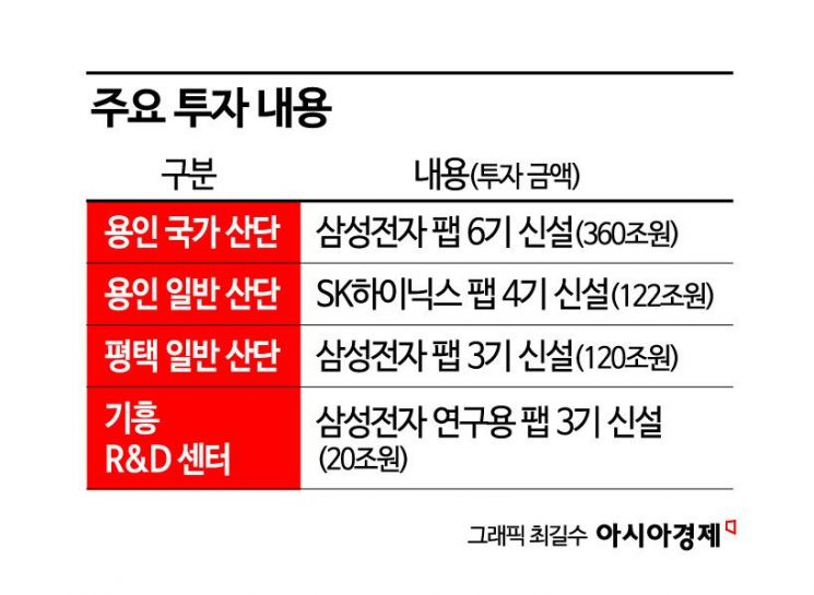
SK Hynix plans to spend 122 trillion KRW on building fabs in the Yongin cluster and creating a win-win ecosystem supporting materials, parts, and equipment. They plan to sequentially construct the 4th semiconductor production line, called a fab, for producing DRAM and next-generation memory semiconductors on a 4.15 million square meter site in Jukneung-ri, Wonsam-myeon, Yongin City. A cooperative complex will also be established to house about 50 related companies producing not only semiconductor materials but also front- and back-end process equipment. Residential facilities for employees working in the cluster, as well as commercial and support facilities, parks, drainage basins, and substations will also be built.
SK Hynix plans to start construction of the first factory in 2025 and complete it in 2027. Each fab is expected to employ about 3,000 people, including 1,400 engineers, 1,000 maintenance staff, and 600 operational personnel. In the four fabs alone, about 12,000 people will work, with an additional 3,000 in R&D and support departments, totaling approximately 15,000 employees active in the semiconductor cluster. Furthermore, about 8,000 workers are expected to be employed in the cooperative complex of 50 companies, making it a high-tech industrial city with around 23,000 semiconductor professionals. SK Hynix plans to intensively develop the Yongin semiconductor cluster not only as a production base for DRAM and next-generation memory but also as a hub for a win-win semiconductor ecosystem.
© The Asia Business Daily(www.asiae.co.kr). All rights reserved.
![From Bar Hostess to Organ Seller to High Society... The Grotesque Con of a "Human Counterfeit" [Slate]](https://cwcontent.asiae.co.kr/asiaresize/183/2026021902243444107_1771435474.jpg)


