Introduction of Glass Substrates Essential for Advanced Packaging
Overcoming Limitations of Plastic Substrate Materials
Research Underway Targeting Commercialization by 2025~2030
Intel has announced the introduction of a new semiconductor substrate to enhance its next-generation advanced packaging technology. The company aims to showcase products in cutting-edge fields such as artificial intelligence (AI) by using glass substrates that reduce package thickness to one-quarter of the existing level while improving power efficiency.
On the 18th, Intel stated that the adoption of glass substrates is essential to improve packaging technology, which has recently emerged as a limitation in fine process technology, and that commercialization of the related technology is imminent.
Babak Sabi, Vice President and General Manager of Intel’s Assembly and Test Technology Development division, said, "After 10 years of research, we have secured leading glass substrate technology for advanced packaging," adding, "We will be able to introduce cutting-edge technology that will benefit major companies and foundry customers for decades to come."
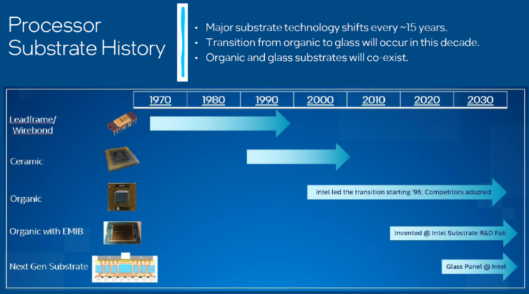 An image explaining the types of processor substrates changing over different eras. Intel predicts that the substrate material will change to glass within the next 10 years. /
 [Image courtesy of Intel]
Intel has recently focused on the limitations of semiconductor substrate materials that have emerged as packaging technology has gradually advanced. Existing semiconductor substrates were made from plastic materials, which are easily deformable and relatively inexpensive. However, these substrates had rough surfaces and difficulties in reducing thickness. There were also issues with substrate warping during the packaging process.
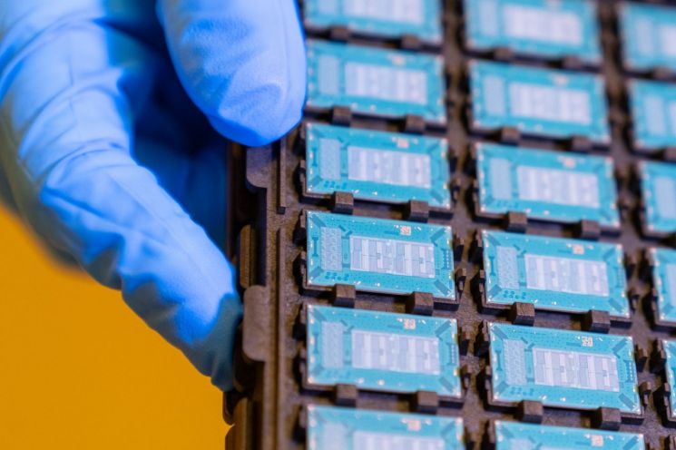
Glass substrates can overcome these limitations of plastic materials. Because they have smooth surfaces and excellent high-temperature resistance, they reduce distortion phenomena that occur when circuits are etched onto the substrate by 50%. This allows for increased chip density, making it possible to reduce package thickness to one-quarter of the existing level. Power consumption can also be reduced.
Intel stated, "The semiconductor industry has entered a heterogeneous era where multiple chiplets are integrated into one package," emphasizing that "glass substrates are an essential step to implement next-generation semiconductors." They also explained, "Glass substrates enable the assembly of chiplet complexes called System-in-Package (SiP)," adding, "This increases assembly yield and allows for the realization of ultra-large form factor packages."
The company has researched glass substrates for over 10 years. It has invested $1 billion in Chandler, Arizona, to establish a research and development (R&D) line for glass substrates, and has secured more than 600 patents related to this technology. Intel plans to introduce products using glass substrates between 2025 and 2030, with initial applications expected in data centers and artificial intelligence (AI).
Intel said, "We are striving to integrate one trillion transistors in a single package by 2030," and added, "We will continue to innovate in advanced packaging fields, including glass substrates, to achieve this goal."
© The Asia Business Daily(www.asiae.co.kr). All rights reserved.
![Clutching a Stolen Dior Bag, Saying "I Hate Being Poor but Real"... The Grotesque Con of a "Human Knockoff" [Slate]](https://cwcontent.asiae.co.kr/asiaresize/183/2026021902243444107_1771435474.jpg)


