Institute for Basic Science Lays Foundation for Commercialization of High-Integration Next-Generation Semiconductors
Domestic researchers have laid the groundwork for the commercialization of highly integrated next-generation semiconductors.
The Institute for Basic Science (IBS) announced on the 5th that the research team led by Lee Young-hee of the Nano-Structure Physics Research Division (Sungkyunkwan University HCR Distinguished Professor), in collaboration with the group leader Yoon Mina from the Oak Ridge National Laboratory in the United States, has developed a new process to fabricate next-generation semiconductor devices without residual substances that cause performance degradation.
To realize next-generation semiconductors with enhanced performance, the development of field-effect transistor (FET) devices with excellent performance is essential. Transition metal dichalcogenides (TMDs), which possess superior physical and electrical properties as well as semiconductor characteristics, have been spotlighted as ideal FET materials to replace silicon. However, despite over a decade of intensive research, residual substances used during the process remain on the devices, hindering performance and posing a barrier to commercialization.
In two-dimensional semiconductor device processes, polymethyl methacrylate (PMMA), an insulator, has traditionally been used as a support material for semiconductor material transfer. However, PMMA residues remaining on TMD semiconductor materials have been a major issue causing device performance degradation. Although various organic materials have been explored to replace PMMA as a support, it has been difficult to avoid electronic and mechanical losses caused by residues.
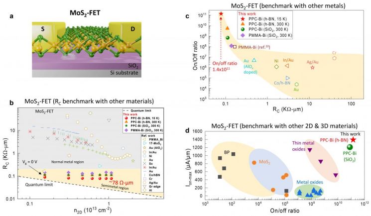
The research team demonstrated that using polypropylene carbonate (PPC) as a support material instead of PMMA can solve this problem. First, they synthesized centimeter-scale molybdenum disulfide (MoS2)-based two-dimensional semiconductor materials suitable for high integration and transferred the semiconductor material using PPC as the support. The single-layer MoS2 devices fabricated in this way contained less than 0.08% of the PPC support material, resulting in almost no performance degradation. Furthermore, they resolved another issue of wrinkling in single-layer semiconductor devices found in previous processes. The team explained that the adsorption energy between PPC and molybdenum disulfide is low, allowing PPC to easily detach from the semiconductor surface, leaving almost no residue.
The MoS2 FET devices produced by the research team exhibited outstanding performance, including a small ohmic contact resistance of 78Ω-μm close to the quantum limit, a large current on/off ratio below 10^11, and a maximum current value below 1.4mA/μm, outperforming any devices developed to date.
Director Lee stated, “The clean two-dimensional device fabrication process we proposed is an ideal platform for applying large-area TMD materials as high-performance electronic devices,” and added, “The two-dimensional semiconductor material transfer technology using PPC support is expected to be widely utilized in the integration of various two-dimensional devices in the future.”
The research results were published in the international journal Nature Nanotechnology (IF 38.3) on the same day.
© The Asia Business Daily(www.asiae.co.kr). All rights reserved.


