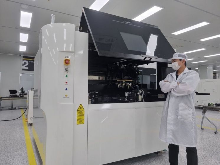
Laser solution platform company LaserCell announced on the 5th that it has succeeded in developing the ‘300mm large-area surface laser core optical system (BSOM) technology’ applicable to AI semiconductor processes and microLED display processes, and will begin full-scale mass production from the second half of this year.
AI semiconductors are packaged forms composed of high-performance chiplet logic semiconductors (Chiplet CPU/GPU) and wide-band ultra-high-speed memory (HBM). To realize this, flip-chip ball grid array (FCBGA) technology, a heterogeneous chip interconnection technology, is required. However, when this technology is applied, the complexity of the technology increases and the final chip area of the package becomes larger, while the chip thickness requires ultra-thinning, raising the issue of bending in AI semiconductors. In addition, many problems arise in the semiconductor bonding process, such as the need to reduce heat input and achieve uniform bonding.
In the case of next-generation microLED display manufacturing processes, the need for new bonding methods through large-area simultaneous pressing heating and minimization of heat input is increasing to improve production yield and minimize performance degradation.
The 300mm large-area variable and fixed surface laser technology that LaserCell is mass-producing this time is optimized for performing large-area bonding processes essential for AI semiconductor and microLED display manufacturing processes, and is evaluated to significantly improve the yield of production processes. In the case of the large-area laser beam BSOM system, it is easy to complete laser beam sizes of more than 300mm in width and length, and through a surface (Area) type light source rather than a typical spot type, the homogenization level of the laser irradiation surface has been successfully achieved at over 90%. The 300mm width and length correspond to 12 inches based on semiconductor wafers.
LaserCell has made it easier to produce surface lasers over 300mm at the required energy density by combining the purely domestic BSOM technology with high-power laser NBOL technology. The implementation of the advanced pressing-type surface laser equipment ‘LC Bonder’ and the non-pressing surface laser equipment ‘LSR’ laser reflow system, which apply surface lasers over 300mm, is expected to play a key role in leveling up Korea’s materials, parts, and equipment technologies in the next-generation laser optical technology field, advanced AI semiconductor industry, and next-generation display industry.
Namseong Kim, CTO leading the R&D headquarters, said, “The 300mm-based surface laser technology developed for the first time in Korea can solve various problems required by the market and achieve differentiated high productivity,” and added, “Based on the synergy of large-area laser core technology that can resolve the recent AI semiconductor shortage situation, high-power laser systems, and process application technologies, we are currently collaborating extensively with several global semiconductor companies and packaging specialists, and will continue to expand these collaborations.”
© The Asia Business Daily(www.asiae.co.kr). All rights reserved.
![Clutching a Stolen Dior Bag, Saying "I Hate Being Poor but Real"... The Grotesque Con of a "Human Knockoff" [Slate]](https://cwcontent.asiae.co.kr/asiaresize/183/2026021902243444107_1771435474.jpg)


