A technology for fabricating high-performance p-type semiconductor devices based on two-dimensional materials, which can be practically used in the next-generation complementary metal-oxide-semiconductor (CMOS) industry applying miniaturization technology, has been developed.
The research team led by Professor Kwon Soon-yong from the Graduate School of Semiconductor Materials and Components and the Department of Materials Science and Engineering at UNIST, in collaboration with Professor Lee Jong-hoon’s team at UNIST, succeeded in fabricating high-performance p-type semiconductor devices using molybdenum ditelluride compound semiconductor (MoTe2).
CMOS is a device where p-type and n-type semiconductors are complementarily connected. It is widely used in everyday electronic devices such as PCs and smartphones due to its low power consumption. Silicon-based CMOS is mainly used, and p-type and n-type semiconductor devices can be implemented through ion implantation processes.
Two-dimensional materials are attracting attention as next-generation semiconductors, but their extremely thin thickness makes their structure easily damaged during the same process.
In particular, two-dimensional materials have the problem of various defects occurring at the interface when forming conventional three-dimensional metal electrodes. Although various studies have been conducted to solve this issue, most research has focused on ‘n-type semiconductors’.
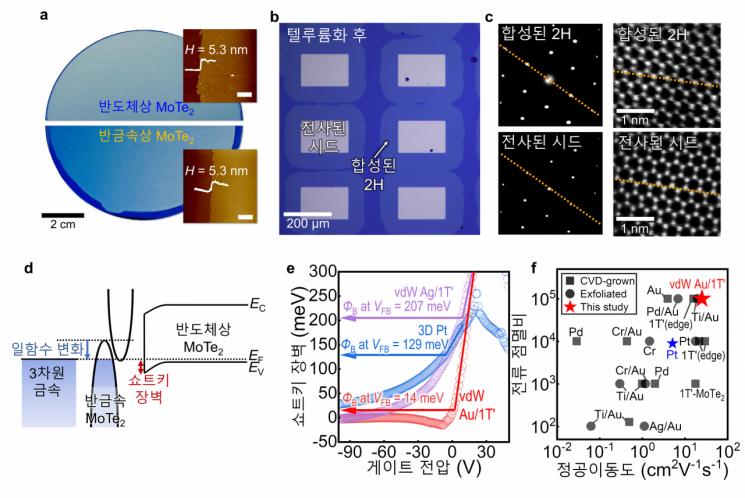 Schematic diagram of the synthesis of large-area molybdenum telluride compound semiconductor (MoTe2) and the implementation of a high-performance p-type transistor device using three-dimensional metal/two-dimensional semimetal electrodes.
Conversely, the research team utilized molybdenum ditelluride compound semiconductor (MoTe2) among ‘p-type semiconductors.’ They developed a technology capable of synthesizing devices over a large 4-inch area using chemical vapor deposition (CVD), a method that creates thin films through chemical reactions.
Based on the developed technology, they fabricated high-performance p-type transistors by utilizing the fact that the work function is modulated when three-dimensional metals are deposited on two-dimensional semi-metals.
They also synthesized high-purity semiconductor thin films of 4-inch size by controlling the synthesis temperature and time. After transferring a semiconductor seed that facilitates phase transition onto the semi-metal thin film and synthesizing at a low temperature below 500℃, they confirmed that high-quality semiconductors are formed in the shape of the seed’s crystal structure.
The research team implemented a new transistor by utilizing the property of modulated work function. This transistor minimizes the barrier layer that blocks the ‘charge carriers,’ which are materials that transport charge.
They also confirmed that the three-dimensional metal acts as a protective layer for the two-dimensional metal, enabling the implementation of transistor array devices with improved yield compared to existing ones.
Jang Sora, a first author and integrated MS-PhD course researcher, explained, “The device fabrication method developed in this study can be applied not only to the two-dimensional semiconductors presented in the paper but also to various two-dimensional materials,” and added, “We hope that the developed two-dimensional materials will be applied to the CMOS industry and contribute to improved integration.”
The research results were published online on August 7 in the international journal Nature Communications.
The research was supported and conducted with funding from the Ministry of Science and ICT’s Korea Research Foundation’s Nano and Materials Technology Development Project and Mid-career Researcher Support Project, the IBS Multidimensional Carbon Materials Research Center, and the UNIST Future Leading Specialized Project.
© The Asia Business Daily(www.asiae.co.kr). All rights reserved.


