Rise of Semiconductor Challenges in the AI Era
Samsung Electronics Boosts Advanced Process Competitiveness with GAA
Full Effort to Secure Customer Support Packaging Technology
"Gate-All-Around (GAA) is an optimized solution for AI semiconductors that implement high performance at low power. We plan to expand 3D packaging technology to GAA by 2025."
Choi Si-young, President of Samsung Electronics Foundry Division, said this on the 4th at the 'Samsung Foundry Forum 2023' regarding Samsung's foundry strategy in response to the AI era. The Samsung Foundry Forum is an event where Samsung Electronics introduces its foundry vision and latest technologies to fabless (semiconductor design) customers. President Choi delivered the keynote speech introducing Samsung Electronics' foundry strategy to prepare for the AI era.
 Choi Si-young, President of Samsung Electronics, is delivering the keynote speech at the 'Samsung Foundry Forum 2023' held at COEX in Seoul on the 4th. / Photo by Samsung Electronics
Samsung Electronics presented two core pillars of its foundry strategy to respond to the AI era: GAA and advanced packaging technology. GAA is a next-generation transistor technology that increases gate area to enhance data processing speed and power efficiency. It overcomes the limitations of the existing transistor structure, FinFET, and is regarded as a game changer in foundry.
Samsung Electronics first introduced GAA technology when it began mass production of the 3-nanometer (nm; 1 nm = one billionth of a meter) process in June last year, the first in the industry. It is pushing forward the next-generation development strategy called 'Easy Transition,' which continues GAA technology to the 2 nm process scheduled for mass production next year and the 1.4 nm process planned for 2027.
Innovation in packaging technology is also a major task. Recently, the semiconductor industry has been developing advanced packaging technologies to improve performance due to the limits of semiconductor fine circuits. Samsung Electronics also expanded related business by establishing the Advanced Packaging (AVP) business team earlier this year.
Samsung formed the 'Multi-Die Integration (MDI) Alliance,' an advanced package consortium with partners from various fields such as memory and testing, and is building an ecosystem for 2.5-dimensional (2.5D) and 3D heterogeneous integration (a packaging technology that allows semiconductors with different functions to operate as one semiconductor). Through this, it provides customers with a state-of-the-art package one-stop turnkey service.
To expand customer support, Samsung also announced plans to expand semiconductor design assets (IP) and establish R&D bases to secure a technological lead. In particular, it is preparing a new research center in Japan following Korea and the United States for advanced technology development, and is broadening the scope of free support for Multi-Project Wafer (MPW) services for R&D cooperation with domestic and international universities and research institutes. MPW is a service that supports prototype production by manufacturing multiple types of semiconductor products on a single wafer.
President Choi said, "Historically, whenever a crisis occurred, society underwent major changes and progressed repeatedly, and at the center of that process was technological innovation," adding, "Semiconductor innovative technology will lead the way to change the world and people's lives."
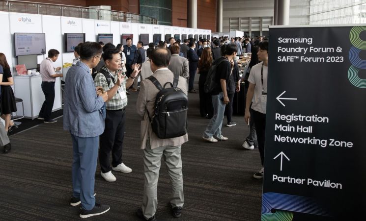 Samsung Electronics' customers and partners are having a conversation at the 'Samsung Foundry/SAFE Forum' held on the 4th at COEX, Samseong-dong. / Photo by Samsung Electronics
Meanwhile, Samsung Electronics previously announced at the 'Samsung Advanced Foundry Ecosystem (SAFE) Forum 2023' that it will support the semiconductor design support kit (PDK) called 'Prime Solution' for legacy processes starting with advanced 2 nm and 3 nm processes in the second half of the year.
© The Asia Business Daily(www.asiae.co.kr). All rights reserved.


