Agreement Ceremony Held on the Afternoon of the 21st
5 More 28-Nanometer Productions and 200 Additional Units
Students at the Korea Advanced Institute of Science and Technology (KAIST) now have significantly expanded opportunities to practice system semiconductor design and fabrication using Samsung Electronics' equipment.
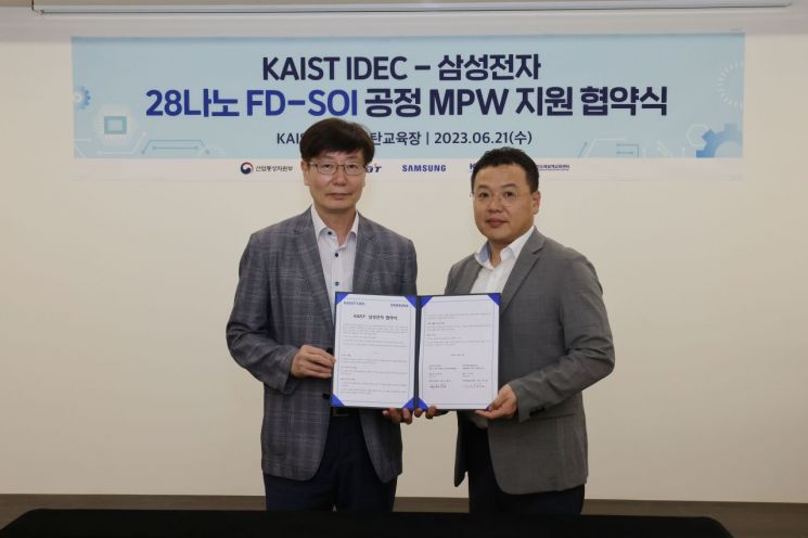 KAIST and Samsung Electronics held a signing ceremony on the afternoon of the 23rd at the IDEC Dongtan Education Center to support additional production of system semiconductors (28nm FD-SOI MPW). (From left) Incheol Park, Director of KAIST IDEC, and Sanghoon Park, Executive Director of Samsung Electronics. Photo by KAIST
On the afternoon of the 21st, KAIST held a signing ceremony for an agreement with Samsung Electronics to expand support for nurturing semiconductor talent through additional system semiconductor (28nm) fabrication support. In this regard, KAIST's Semiconductor Design Education Center (IDEC) has been conducting the "Next-Generation System Semiconductor Design Talent Development Project" since 2021 with government support. This project provides a specialized education program covering semiconductor chip design to fabrication for master's and doctoral students nationwide, with a total government funding of 17 billion KRW over five years.
Specifically, since 2021, KAIST has collaborated with Samsung Electronics to offer students opportunities to fabricate chips using the 28nm logic process. Samsung Electronics had planned to conduct 10 fabrication runs by 2026, supporting the production of a total of 400 system semiconductor chips.
However, on this day, KAIST and Samsung Electronics signed a new agreement to provide five additional fabrication runs, supporting the production of 200 more chips. In other words, during the period of the "Next-Generation System Semiconductor Design Talent Development Project," a total of 15 fabrication runs will be conducted, offering opportunities to design and fabricate 600 chips.
Semiconductor chip fabrication is a crucial process where graduate students apply their theoretically designed schematics onto wafers to create physical chips. This allows verification of design suitability through experiments using actual chips. However, commissioning chip fabrication through semiconductor foundries typically costs tens of millions to hundreds of millions of KRW, making such opportunities difficult to obtain.
Park In-cheol, director of KAIST IDEC, stated, "Our talent development project serves as an important foundation for many graduate students nationwide in semiconductor design to directly participate in semiconductor fabrication processes, gaining practical experience and project participation credentials."
© The Asia Business Daily(www.asiae.co.kr). All rights reserved.
![Clutching a Stolen Dior Bag, Saying "I Hate Being Poor but Real"... The Grotesque Con of a "Human Knockoff" [Slate]](https://cwcontent.asiae.co.kr/asiaresize/183/2026021902243444107_1771435474.jpg)


