Publication of Related Research Results in a World-Renowned Academic Journal
Samsung Electronics SAIT (formerly the Advanced Institute of Technology) has developed system semiconductor implementation technology that applies next-generation semiconductor materials to enhance performance and power efficiency. The company aims to increase the commercialization potential of the new transistor technology and establish it as a core driver for Samsung Electronics' foundry (semiconductor contract manufacturing) business.
On the 1st, Samsung Electronics announced the achievement through internal research and posted the news on its semiconductor newsroom. It also added that the research paper was published in the world-renowned academic journal 'Nature Electronics.'
The research paper involved SAIT employees as first authors, corresponding authors, and co-authors. Employees from Samsung Electronics DS Division Semiconductor Research Institute were also listed as co-authors.
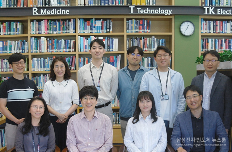 Samsung Electronics SAIT researchers who developed system semiconductor implementation technology that enhances performance and power efficiency using next-generation semiconductor materials /
 [Photo by Samsung Electronics Semiconductor Newsroom]
The research team focused on the issue of leakage current that occurred during the process of enhancing performance, even as the performance of system semiconductors, which perform data computation and processing functions within computing systems, becomes increasingly important with the spread of artificial intelligence (AI) services.
To improve system semiconductor performance, transistors must be miniaturized and integration density increased. However, in this process, the insulating layer within the transistor also becomes thinner, leading to an increase in leakage current.
The researchers confirmed that replacing the high-k dielectric material used in the insulating layer with a new material, ferroelectric material, can reduce leakage current. By utilizing the characteristics of ferroelectric materials, it is possible to reduce operating voltage without increasing leakage current, which, according to the researchers, leads to a reduction in transistor power consumption.
In fact, semiconductors using ferroelectric materials were able to reduce power consumption by up to 33% compared to semiconductors using conventional high-k dielectric materials in the same structure.
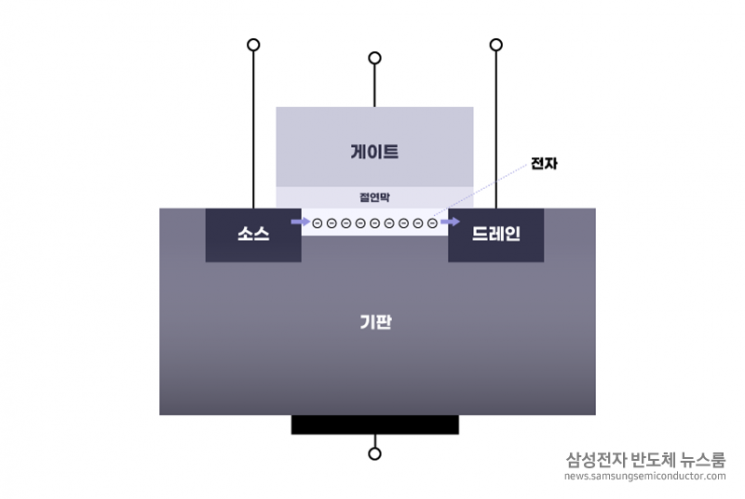 Internal image of transistor structure (nMOSFET) /
 [Image source=Samsung Electronics Semiconductor Newsroom]
The research team stated that it is significant to have verified for the first time in the world the commercialization potential of a new transistor structure called 'NCFET' that utilizes the negative capacitance (NC) effect. They also added that this technology can be applied to all transistor structures, including existing three-dimensional (3D) structure transistors such as FinFET and Gate-All-Around (GAA).
Sanghyun Cho, a researcher at Samsung Electronics SAIT (co-first author), said, "In addition to experimentally verifying the NC effect of ferroelectric materials, we simultaneously confirmed the feasibility of thickness miniaturization, reliability assurance, and adjustment of the NC operating range. This is significant as it confirms the commercialization potential of next-generation low-power, high-performance system semiconductor devices."
He added, "We will further improve ferroelectric thin film growth and device technology," and "We expect this to become a core future technology for our foundry (semiconductor contract manufacturing) business."
© The Asia Business Daily(www.asiae.co.kr). All rights reserved.
![Clutching a Stolen Dior Bag, Saying "I Hate Being Poor but Real"... The Grotesque Con of a "Human Knockoff" [Slate]](https://cwcontent.asiae.co.kr/asiaresize/183/2026021902243444107_1771435474.jpg)


