SK Hynix Considers Fab Construction Options with Allies
"Global Fab Remapping Underway... Will Share at MWC if Necessary"
[Asia Economy Reporter Kim Pyeonghwa] Park Jeong-ho, Vice Chairman of SK Hynix, said that the ongoing semiconductor production cuts would not be on a large scale. He also added that they would closely monitor and respond to issues at global hubs, including the packaging facility to be established in the United States.
After participating in the academic symposium commemorating the opening of the Doheon Academy held at the Korea Press Center on the afternoon of the 15th, Vice Chairman Park told reporters, "When supply is excessively high, we consider slowing down, but in reality, excessive production cuts are not good from a competitiveness perspective," adding, "We are taking both into account and believe it will be difficult to make drastic cuts."
Regarding concerns arising from the recent specification of guardrail provisions related to the U.S. semiconductor support law and its impact on operations of production facilities in China, he said, "It seems necessary to make efforts to alleviate the concentration in Asia, and I think we should respond accordingly."
He continued, "Considering the investment capacity during a downturn, shouldn't we look at options such as jointly building fabs with other countries or allies?" and added, "Asking for more time does not seem like a constant." This statement implies the limitations of seeking short-term cooperation from the U.S. through a one-year grace period.
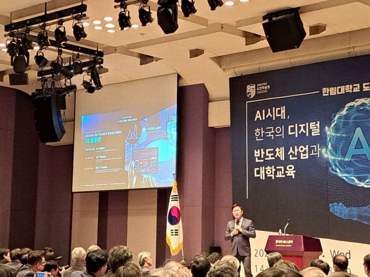 Park Jung-ho, Vice Chairman of SK Hynix, is delivering the keynote speech at the academic symposium commemorating the opening of the Doheon Academy. /
 Photo by Kim Pyeong-hwa
When asked by reporters about the progress of the advanced semiconductor packaging plant and research and development (R&D) center to be established in the U.S., Vice Chairman Park replied, "The R&D center seems to be taking time, and we are currently looking for a site for advanced packaging." Earlier, SK Hynix announced plans to invest $15 billion to introduce these facilities in the U.S. The advanced packaging plant site is expected to be selected within the first half of the year.
He also said, "We are remapping our global fabs again," adding, "When the time is right, we will be able to discuss this at events such as MWC." SK Hynix explained that Vice Chairman Park’s remark about remapping means they intend to closely monitor issues at each global production base.
© The Asia Business Daily(www.asiae.co.kr). All rights reserved.
![Clutching a Stolen Dior Bag, Saying "I Hate Being Poor but Real"... The Grotesque Con of a "Human Knockoff" [Slate]](https://cwcontent.asiae.co.kr/asiaresize/183/2026021902243444107_1771435474.jpg)


