Professor Hong Young-jun of Sejong University and International Collaborative Research Team
Published in International Journal Nature on the 2nd
Domestic researchers have developed a core technology for manufacturing ultra-fine full-color micro LED (light-emitting device composed of semiconductor p-n junctions) pixels, a key technology for microdisplays that realistically implement virtual and augmented reality.
The National Research Foundation of Korea announced on the 9th that a joint research team led by Professor Hong Young-jun of Sejong University succeeded in developing a new epitaxy technology that allows easy detachment from wafers and a manufacturing technology for ultra-high-density arrays of vertical micro LED pixels using this method. Epitaxy refers to the process of manufacturing semiconductor devices (such as transistors and LEDs) with single crystallinity on a wafer.
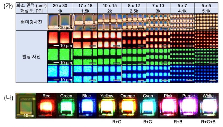 (a) Front-lit photos of vertical pixel micro LEDs produced at resolution levels ranging from 1,000 PPI to 5,100 PPI in red, green, and blue. High-density implementation is easy due to the vertically stacked pixel structure. (b) Photos of various emitted colors and white light created by adjusting the current applied to red, green, and blue LEDs.
As mobile devices and virtual and augmented reality technologies advance, competition to develop ultra-high-resolution, ultra-realistic, and ultra-compact displays that provide users with high immersion without spatial constraints is fierce. However, the existing method of making LEDs into small chips and transferring them to create displays faces limitations in implementing high-resolution displays because the smaller the chip, the lower the transfer position accuracy and success rate. To separate LEDs chemically strongly bonded to the wafer, chemical etching or high-power lasers must be used, making it difficult to separate LEDs over large areas with high yield, and requiring significant process costs and time.
The research team developed a new concept of remote and van der Waals epitaxy method by coating the wafer surface with nanomaterials and then manufacturing single-crystal semiconductors. They manufactured LEDs so that red, green, and blue light-emitting LED layers could be easily detached from the wafer in the form of a large-area membrane (a very thin film with a thickness of several hundred nanometers (nm) to several micrometers (μm)) and utilized this for ultra-fine pixel fabrication. Along with this, the red, green, and blue light-emitting LED membranes separated from the wafer were stacked vertically like pancakes, and pixels were patterned to a size of 4 micrometers using a high-precision photolithography process, producing ultra-fine vertical pixels that realize full natural color at about 5100 PPI (pixels per inch). The wafer from which the LEDs were detached can repeatedly produce LEDs of the same quality, which is expected to reduce display manufacturing costs.
The research team explained, “Stacked micro LED vertical pixels can improve pixel density by at least three times compared to the existing horizontal side-by-side arrangement, making them suitable for applications and manufacturing of high-resolution, ultra-realistic AR, XR, and metaverse displays.”
The research results were published in the international academic journal Nature on the 2nd.
© The Asia Business Daily(www.asiae.co.kr). All rights reserved.


