US Bans Semiconductor EDA Tool Exports to China
China Responds by Expanding Domestic EDA
Scalability Essential as EDA Ecosystem Barriers Grow

[Asia Economy Reporter Kim Pyeonghwa] As the United States increases regulatory measures against China's semiconductor rise, the export ban on semiconductor electronic design automation (EDA) tools is also drawing attention. Since EDA tools are essential for semiconductor design, China is striving to develop domestic EDA tools and promote localization in response. However, industry insiders believe that due to the characteristics of EDA tools and the challenges of the related market, China's attempts will not be easy.
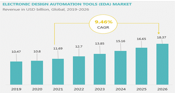
According to the semiconductor industry on the 23rd, as the semiconductor market grows, the importance of EDA tools is highlighted, leading to a tug-of-war between the US and China. EDA tools are software programs used for circuit design, error detection, and problem-solving through simulation before semiconductor manufacturing. As semiconductor performance advances and demand increases, error-free design and reduced production time become crucial, increasing the use of EDA tools. Especially, as the semiconductor design market expands, the demand for EDA tools is on the rise. Market research firm EMIS forecasts that the related market will grow from $11.7 billion last year to $18.3 billion by 2026, with an average annual growth rate of 9.46%.
The US, considering EDA tools as core to the semiconductor industry, uses them as a means to sanction China. In August, the US banned the export of EDA tools necessary for designing integrated circuits (ICs) with gate-all-around (GAA) FET structures to China. Since GAAFET is used in cutting-edge processes below 3 nanometers (nm; 1 nm = one billionth of a meter), the US intends to cut off China's advanced semiconductor development. Previously, when increasing sanctions against China's Huawei, the US also blocked EDA supplies to Huawei and its subsidiaries.
In response to these sanctions, China is making efforts to expand domestic EDA tools. This month, China announced a semiconductor industry development plan in Shenzhen, offering subsidies of up to 10 million yuan to companies using domestic EDA tools. China is also actively fostering EDA tool companies. According to the Korea Trade-Investment Promotion Agency (KOTRA), as of 2020, there are 49 Chinese EDA tool companies, including Empyrean and Primarius. From 2018 to 2020, the local market share of China's EDA market sales increased from 6% to 11%.
Kim Da-in of KOTRA's Shanghai Trade Center explained in a related report, "China's EDA design direction will develop towards intelligent trends by reducing human and material resources due to talent pool limitations," adding, "The central and local governments in China are also announcing various policies to build core technologies like EDA."
Industry experts and semiconductor professionals believe China's attempts are inevitably limited. This is because the market where Chinese EDA tools can expand is not broad in terms of scalability and versatility. According to market research firm TrendForce, in the global EDA tool market last year, three companies?US-based Synopsys (32%), Cadence (30%), and Germany's Siemens EDA (13%)?accounted for 75% of the market share. These companies have been operating EDA tool businesses for over 30 years and have a solid customer base. The EDA market itself has high entry barriers, and due to the nature of the EDA tool business, continuous cooperation with numerous chip design and wafer manufacturers is necessary, making ecosystem formation essential.
Professor Eom Jae-cheol of Youngjin College's Semiconductor Electronics Department said, "In terms of performance and scalability, US commercial tools are naturally better, but since supply is cut off, China is trying to use domestic tools as a last resort," adding, "Although there are domestic companies, it will be difficult to suddenly reach the technological level."
TrendForce recently predicted that as Chinese semiconductor IC design companies gradually move toward 4 nm processes, by 2025, the impact of the US sanctions on 3 nm EDA tools against China will become visible. This could delay the development schedules of local IC design companies and hinder industrial development.
On the other hand, some view that China could achieve partial success. Despite various difficulties caused by US sanctions, China's potential is greater than expected, and its active technological investments might enable long-term EDA tool self-reliance. Recently, attempts to integrate artificial intelligence (AI) technology into the advancement of EDA tools have been active, and China's ability to enhance AI technology based on vast data is also a variable.
A software industry insider said, "China's software and AI technology have improved significantly compared to the past," adding, "Related companies receive national support and can freely use massive amounts of data, which can improve performance with data necessary for AI training."
© The Asia Business Daily(www.asiae.co.kr). All rights reserved.


