Samsung Foundry Forum 2022 Held in Silicon Valley, USA
Advancing Cutting-Edge Process and Packaging Technology Innovation, Diversifying Applications by Process
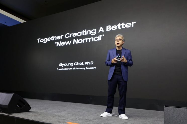 Choi Si-young, President of Samsung Electronics, is giving a presentation at the 'Samsung Foundry Forum 2022'. / Provided by Samsung Electronics
[Asia Economy Reporter Kim Pyeonghwa] On the 3rd (local time), Samsung Electronics held the 'Samsung Foundry Forum 2022' in Silicon Valley, USA, unveiling new foundry technologies and business strategies. The company also announced plans to mass-produce 1.4-nanometer (nm, one-billionth of a meter) chips by 2027.
This year's forum was held offline for the first time in three years. About 500 attendees including fabless customers, partners, and collaborators participated. At the event, Samsung Electronics emphasized strengthening its foundry business competitiveness by leading foundry technology innovation, providing optimized processes for various applications, offering customized customer services, and securing stable production capacity.
Choi Si-young, head of Samsung Electronics' Foundry Business Division, stressed, "The success of our customers is the reason for the existence of Samsung Electronics' Foundry Business Division," adding, "Samsung Electronics will become a new standard in the foundry industry as a partner creating a better future."
Strengthening Leading-edge Process Leadership through Foundry Technology Innovation... Mass Production of 1.4nm by 2027
At the forum, Samsung Electronics announced accelerating innovation in leading-edge foundry processes and the development of next-generation packaging stacking technologies. Samsung was the first in the world to mass-produce FinFET transistors in 2015. In June this year, it also became the first to start mass production of the 3nm first-generation process applying Gate-All-Around (GAA) transistor technology.
Samsung Electronics is expanding 3nm applications based on its advanced mass production know-how. It plans to continue innovating GAA-based process technology, introducing 2nm in 2025 and 1.4nm processes in 2027.
Samsung is also accelerating the development of 2.5D and 3D heterogeneous integration packaging technologies. While applying its proprietary MBCFET structure to the 3nm GAA technology, Samsung will also provide 3D IC solutions to offer high-performance semiconductor foundry services.
Since the successful launch of high-bandwidth memory HBM2 in 2015, Samsung has continuously innovated packaging stacking technologies such as I-Cube (2.5D) in 2018 and X-Cube (3D) in 2020. I-Cube is a 2.5D package technology that places logic and HBM on a silicon interposer. X-Cube is a 3D package technology that stacks multiple chips thinly in wafer form.
Samsung plans to mass-produce u-Bump type X-Cube in 2024 and introduce Bump-less type X-Cube in 2026. u-Bump allows more I/Os to be packed compared to conventional bumps, enabling higher data processing. Bump-less eliminates bumps in packaging, allowing even more I/O insertion and thus greater data processing capacity than u-Bump.
Expanding HPC, 5G, Automotive, etc. to Over 50% by 2027
Samsung Electronics plans to actively target high-performance low-power semiconductor markets such as high-performance computing (HPC), automotive semiconductors, 5th generation mobile communication (5G), and Internet of Things (IoT), aiming to increase the sales proportion of non-mobile product groups to over 50% by 2027.
Following the world's first mass production of 3nm process-based HPC products in June, Samsung will expand the 4nm process to HPC and automotive applications. It also plans to develop various processes for eNVM and RF to provide foundry services tailored to customer demands.
Samsung is expanding its 28nm automotive eNVM solution currently in mass production to 14nm in 2024 and is developing technology for an 8nm eNVM solution in the future.
Samsung is also expanding its RF process services. After successfully mass-producing 14nm RF processes, Samsung achieved the world's first mass production of 8nm RF products and is currently developing 5nm RF processes.
Expanding SAFE Ecosystem to Strengthen Customized Customer Services
As of this year, Samsung Electronics provides over 4,000 IPs with 56 IP partners. It also collaborates with 9 Design Solution Partners (DSP) and 22 Electronic Design Automation (EDA) partners. Additionally, it offers packaging services to 9 cloud service partners and 10 OSAT partners.
Samsung plans to strengthen customized services that combine enhanced performance and functionality, quick delivery, and price competitiveness to discover new fabless customers and actively attract new clients such as hyperscalers (large-scale data center operators) and startups.
At the SAFE Forum held on the 4th (local time), Samsung will introduce new foundry technologies and strategies together with partners in EDA, IP, OSAT, DSP, and Cloud sectors.
Timely Response to Customer Needs through 'Shell First' Line Operation
Samsung plans to expand leading-edge process production capacity more than threefold by 2027 compared to this year to actively meet customer demands. It operates leading-edge foundry manufacturing lines in Pyeongtaek, Hwaseong, and Taylor, USA, while mature processes are mass-produced in Hwaseong, Giheung, and Austin, USA.
Samsung will respond quickly and flexibly to market demand through 'Shell First' line operation. 'Shell First' means preemptively constructing cleanrooms and securing stable production capacity through flexible facility investments linked to future market demand, thereby actively responding to customer needs. Samsung plans to proceed with the second line investment at the Taylor foundry following the 'Shell First' approach after the first line. There is also potential for expanding global lines domestically and abroad in the future.
Meanwhile, Samsung Electronics will sequentially hold Samsung Foundry Forums starting from Silicon Valley, USA on the 3rd (local time), then Europe (Munich, Germany) on the 7th, Japan (Tokyo) on the 18th, and Korea (Seoul) on the 20th. Customized solutions for each region's customers will be introduced. For global customers unable to attend offline, the event content will be available online starting from the 21st.
© The Asia Business Daily(www.asiae.co.kr). All rights reserved.


