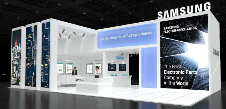
Samsung Electro-Mechanics Exhibits High-Performance, High-Density, Ultra-Slim Semiconductor Package Substrates for 5G, AI, and Automotive Applications
LG Innotek Introduces Global No.1 Products Including Wireless Frequency Package Substrates and Chip-on-Film
[Asia Economy Reporter Kim Pyeonghwa] Samsung Electro-Mechanics and LG Innotek will participate in the largest domestic substrate exhibition starting on the 21st of this month. Both companies will showcase products related to high-performance Flip Chip Ball Grid Array (FC-BGA) substrates, which connect semiconductor chips to main substrates, demonstrating their technological capabilities. Samsung Electro-Mechanics will focus on exhibiting high-performance FC-BGA with high technical difficulty for servers, while LG Innotek will unveil a new FC-BGA product that reduces warpage in digital transformation (DX) processes.
Samsung Electro-Mechanics Server FC-BGA Highest Difficulty Product... Mass Production Scheduled by Year-End
Samsung Electro-Mechanics will participate in the 'International PCB and Semiconductor Packaging Industry Exhibition (KPCA Show 2022)' held from the 21st to the 23rd at Songdo Convensia, Incheon Metropolitan City, revealing next-generation semiconductor package technology. The KPCA Show is the largest domestic substrate exhibition with participation from domestic and international substrate, material, and equipment companies. Over 180 companies from home and abroad will share the latest technology trends.
As a semiconductor package substrate company, Samsung Electro-Mechanics will exhibit high-performance, high-density, ultra-slim next-generation semiconductor package substrates at this exhibition. Semiconductor package substrates are products that connect highly integrated semiconductor chips to mainboards, transmitting electrical signals and power. Due to the high performance of semiconductors in AI and automotive electronics, package substrates require advanced technologies such as increased internal layers, fine circuit implementation, and precise interlayer alignment.
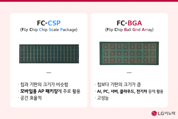
Samsung Electro-Mechanics plans to focus on exhibiting high-performance FC-BGA for servers and other applications. FC-BGA is a highly integrated package substrate that connects semiconductor chips and package substrates using the flip chip method, enhancing electrical and thermal characteristics. It is a high-spec product mainly used in central processing units (CPU), graphics processing units (GPU), and other components with heavy electrical signal exchange. Among these, server FC-BGA has the highest technical difficulty. The server FC-BGA measures 75x75 mm in size to support high-speed signal processing, which is four times the size of general FC-BGA, and implements more than 20 internal layers, twice that of general products, making it the most challenging product. Samsung Electro-Mechanics plans to start production of server FC-BGA by the end of the year.
Samsung Electro-Mechanics will also exhibit ultra-small, high-density semiconductor substrates for mobile IT. They will introduce Flip Chip Chip Scale Package (FCCSP) with the coreless process that removes the core (internal support layer) inside the semiconductor substrate, reducing thickness by 50% compared to existing products, and System in Package (SiP) that embeds multiple semiconductor chips and passive components such as MLCCs inside the package substrate.
Jang Deokhyun, President of Samsung Electro-Mechanics, said, "Next-generation package substrates will become platforms that integrate all systems."
FC-BGA Substrate New Product, Manufactured to Customer-Desired Thickness... Minimizing Warpage
LG Innotek will showcase three innovative products at the KPCA Show: Flip Chip Ball Grid Array (FC-BGA) substrates, package substrates, and tape substrates.
LG Innotek's new FC-BGA substrate product, scheduled for mass production next year, features the application of various DX technologies such as AI and digital twin in the development process. Depending on the application, substrates can be manufactured in various thicknesses desired by customers, including coreless, thin core, and thick core types. This is the industry's first case of applying coreless technology, previously used in radio frequency system-in-package (RF-SiP) substrates, to FC-BGA substrates. The product also minimizes critical warpage (the bending of substrates caused by heat and pressure during manufacturing). Warpage is increasing proportionally with the substrate area as FC-BGA substrates grow larger due to high-performance and high-spec semiconductors.
LG Innotek will also unveil semiconductor substrates used in the latest mobile wireless communication front-end modules, application processors (AP), and memory. They will exhibit substrates for RF-SiP, which holds the world's number one market share, as well as substrates for Flip Chip Chip Scale Package (FCCSP) and Chip Scale Package (CSP). Additionally, they will introduce Chip on Film (COF), which holds the world's number one market share, 2Metal Chip on Film (2Metal COF), and Chip on Board (COB). COF and 2Metal COF connect display panels of smartphones, TVs, and main substrates, while COB is used in credit cards and passports. LG Innotek applies its ultra-fine process technology to Chip on Film.
Son Gildong, Executive Vice President and Head of Substrate Material Business Division at LG Innotek, said, "Based on our global market-leading capabilities, we will rapidly expand our substrate material business from mobile and display to PC/server, communication/network, metaverse, and automotive sectors. We will continuously introduce new substrate material products to innovate customer experiences."
© The Asia Business Daily(www.asiae.co.kr). All rights reserved.
![From Hostess to Organ Seller to High Society... The Grotesque Scam of a "Human Counterfeit" Shaking the Korean Psyche [Slate]](https://cwcontent.asiae.co.kr/asiaresize/183/2026021902243444107_1771435474.jpg)


