Vice Chairman Lee Jae-yong's Possible Attendance
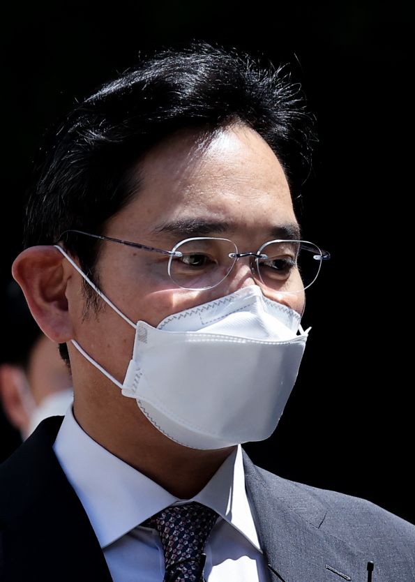
[Asia Economy Reporter Park Sun-mi] Samsung Electronics will hold a groundbreaking ceremony for its semiconductor research and development (R&D) complex on the 19th at its Giheung Campus in Gyeonggi Province. There is a possibility that Samsung Electronics Vice Chairman Lee Jae-yong will attend the groundbreaking ceremony as his first official event following the special pardon on August 15th, Liberation Day.
According to the industry on the 18th, Samsung Electronics will hold the groundbreaking ceremony for the R&D complex at the Giheung Campus in Yongin City on the 19th. The ceremony will be attended by Kyung Kye-hyun, head of the Semiconductor (DS) Division, along with other presidents and business division heads. Although Samsung Electronics plans to conduct the ceremony as an internal event, there is considerable attention on Vice Chairman Lee’s first steps after being reinstated by the August 15th special pardon, leaving open the possibility that he will attend the groundbreaking ceremony.
The R&D complex to be established within the Giheung Campus is expected to serve as a research hub for developing new technologies such as NAND flash, foundry (semiconductor contract manufacturing), and system semiconductors. This will be the first time in eight years since Samsung Electronics established the Device Solution Research (DSR) center at its Hwaseong site in Gyeonggi Province in 2014 that it has built a new R&D center domestically.
Vice Chairman Lee emphasized the importance of securing technology by stating to reporters immediately upon arriving at the airport after his European business trip in June, "First is technology, second is technology, and third is technology."
© The Asia Business Daily(www.asiae.co.kr). All rights reserved.


