Full-Scale Revenue from 3nm Process in Foundry Market This Year
Samsung, Which Started First...Yield Issues to Be Resolved Soon
Aiming to Narrow Market Share Gap with Industry Leader TSMC
[Asia Economy Reporters Sunmi Park, Hyunseok Yoo] Samsung Electronics has officially announced the world's first mass production of 3nm (nanometer, one billionth of a meter) semiconductors. This is faster than TSMC, the world's number one foundry (semiconductor contract manufacturing) market leader, making Samsung the first to produce and supply products with 3nm process-applied semiconductors. This 3nm process is evaluated as Samsung's 'new weapon' to catch up with TSMC and fend off Intel's pursuit.
3nm Process Foundry Service 'World's First'
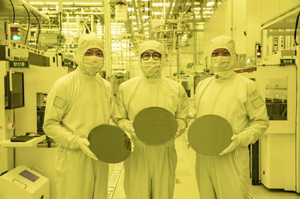
On the 30th, Samsung Electronics announced that it has started initial mass production based on the 3nm foundry process applying Gate-All-Around (GAA) technology, the world's first. The 3nm process is the most advanced technology among semiconductor manufacturing processes.
In particular, Samsung Electronics has applied the next-generation GAA technology for the first time in the world, where the gate surrounds all four sides of the channel through which current flows in the transistor that constitutes the semiconductor. Samsung Electronics is currently the only company worldwide offering 3nm process foundry services applying the next-generation transistor structure GAA technology.
Samsung Electronics' 1st generation 3nm GAA process reduces power consumption by 45% and improves performance by 23% compared to the existing 5nm FinFET process. The area is reduced by 16%. The upcoming 2nd generation GAA process is expected to reduce power consumption by 50%, improve performance by 30%, and reduce area by 35%, allowing more functions and higher performance in semiconductors.
Samsung Electronics stated that after initial production of high-performance computing (HPC) system semiconductors using the 3nm process, it plans to expand to mobile system-on-chip (SoC) and others.
Meanwhile, Samsung Electronics did not disclose the yield when officially announcing the 3nm semiconductor mass production. Generally, the semiconductor industry considers a yield of about 80-90% necessary for stable mass production and securing customers. It is reported that Samsung has not yet secured this level of yield in the 3nm process. However, an agreement has been reached with customers to start mass production at the current yield level, with plans to rapidly improve yield alongside mass production.
Choi Si-young, President of Samsung Electronics' Foundry Business Division, said, "Samsung Electronics, which has rapidly grown by proactively introducing new technologies such as 'High-K Metal Gate,' FinFET, and Extreme Ultraviolet (EUV) lithography as the first in the foundry industry, is now providing the world's first 3nm foundry service applying GAA technology." He added, "We will continue to actively develop differentiated technologies and build a system to quickly improve process maturity."
Significance of 3nm Mass Production and Future Challenges
Samsung Electronics' start of the world's first 3nm semiconductor mass production means it has the technological capability to produce the most challenging advanced products first. Recently, Vice Chairman Lee Jae-yong, who emphasized 'technology management,' has secured a 'super-gap' not only in memory but also in foundry (semiconductor contract manufacturing). If yield (the ratio of actual good products produced to design) is properly secured, reducing market share gap with TSMC, the foundry industry leader by sales, is only a matter of time. In the foundry business structure, differences in process technology directly affect the volume of orders from customers, making it a key factor. This raises the possibility of achieving the 'No.1 system semiconductor by 2030' goal set by Vice Chairman Lee to a higher level.
◆Next-generation core technology 3nm, Samsung 'Seizes the Initiative' = In semiconductors, the nanometer refers to the circuit linewidth; the shorter the linewidth, the more efficient and higher performance the semiconductor can be. This also increases productivity. Orders naturally concentrate on those who first adopt advanced designs. Samsung Electronics entering 3nm semiconductor mass production earlier than competitors carries significant meaning that could change the global semiconductor market trend.
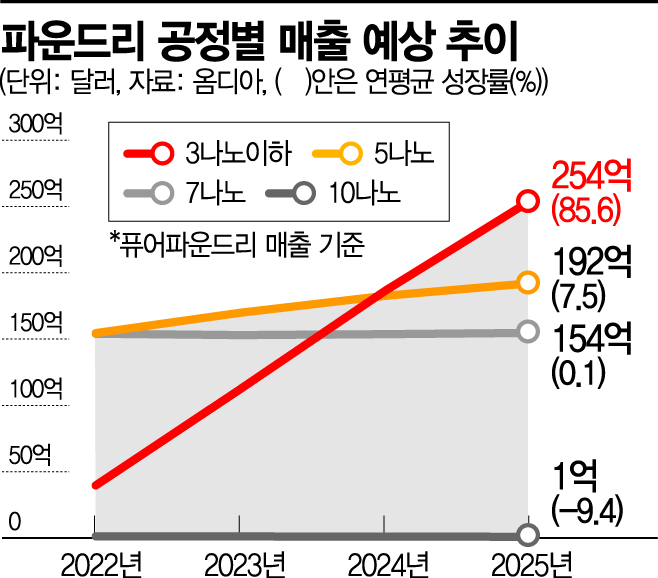
With Samsung Electronics taking the 'first step,' 3nm process sales in the foundry market are expected to accelerate this year. According to market research firm Omdia, sales of processes below 3nm will start at about $3.971 billion this year, growing to $11.239 billion in 2023, $18.644 billion in 2024, and $25.405 billion in 2025, with an average annual growth rate of 85.6%.
For the 5nm process, which is a lower step than 3nm, sales this year are estimated at $15.452 billion, the largest share among all processes. However, its average annual growth rate is only 7.5% until 2025, with sales expected to reach about $18.263 billion in 2024. This means 3nm process sales will surpass it. Samsung Electronics and TSMC are currently the only companies in the world to introduce ultra-fine processes below 10nm. The winner will be decided by who first dominates the 3nm and below processes, where sales volume will exponentially increase.
To overcome the limits of fine processes, Samsung Electronics has proactively introduced next-generation technology, applying the industry's first Gate-All-Around (GAA) technology in this 3nm process. It plans to mass-produce 2nd generation 3nm products next year and 2nm products in 2025.
Competitor TSMC plans to start mass production of 3nm process based on FinFET in the second half of this year. However, even if Samsung and TSMC start the same 3nm process this year, Samsung's GAA technology is evaluated as superior to TSMC's FinFET technology in performance and power consumption. If Samsung succeeds in improving yield, securing customers will be more advantageous.

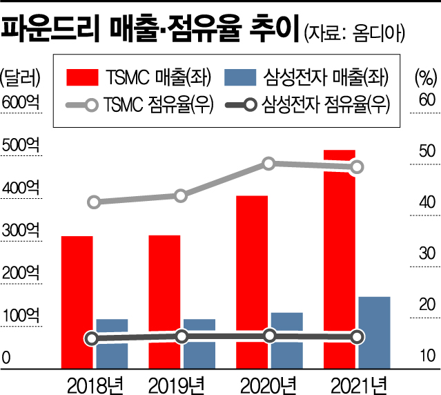
◆Experts: "Yield will improve over time" = Industry experts believe Samsung Electronics' foundry super-gap technology will play a significant role in reducing market share differences with TSMC. According to Omdia, Samsung Electronics' foundry division's sales last year were about $16.9 billion, with a market share of about 16.3%. This is far behind TSMC's $51.3 billion sales and 49.5% market share. However, compared to $11.7 billion in 2018 when Samsung's foundry division started independent sales tracking, it has achieved an average annual growth rate of about 13%, laying the groundwork to narrow the market share gap with TSMC through this 3nm mass production.
A Samsung Electronics official explained, "Foundry is an order-based industry, and growth is possible only by securing customers. Last year, the number of foundry customers exceeded 100, more than tripling compared to 30 customers when the foundry division was separated in 2017. The goal is to secure more than 300 customers by 2026."
With the application of GAA technology, the effect of attracting customers by overcoming the limitations of the existing FinFET process can be expected. Currently, fabless companies (semiconductor design companies) have limited choices between Samsung Electronics and TSMC for orders. Global fabless companies designing mobile APs are actively working to secure as much advanced process capacity as possible.
Professor Park Jae-geun of Hanyang University's Department of Convergence Electronics Engineering said, "The fact that Samsung started mass production earlier than TSMC in the advanced 3nm process itself is meaningful," adding, "Since GAA technology was also applied first, companies like Qualcomm, Nvidia, and Intel, which had concentrated orders with TSMC, will turn their attention to Samsung." He continued, "Although yield may be low at the initial stage of mass production, it is a problem that can improve in a few months. Because Samsung started first, the yield stabilization period will come earlier than TSMC, ultimately contributing to narrowing the market share gap with TSMC."
An Ki-hyun, Executive Director of the Korea Semiconductor Industry Association, also explained, "Samsung has secured a definite technological leadership position by starting the 3nm process applying GAA technology, which TSMC is also attempting, first," adding, "Yield is a problem that can be overcome over time."
© The Asia Business Daily(www.asiae.co.kr). All rights reserved.


