Samsung Competes with TSMC for 17 Years
Brief Lead at 10nm
Lost Lead Again at 7nm
'Counterattack' with 3nm New Technology Mass Production
 Samsung Electronics and TSMC have been competing technologically for dominance in nanometer (nm) fine process technology. / Photo by Jin-Kyung Lee, Asia Economy
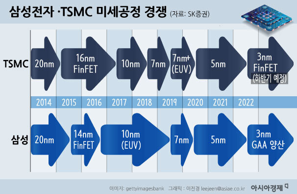
[Asia Economy Reporter Lim Juhyung] As Samsung Electronics has become the world's first to begin mass production of 3-nanometer (nm) semiconductors, the 'fine process competition' in the foundry industry is expected to intensify. Since 2005, Samsung has been engaged in a fierce technological race with Taiwan's TSMC, the industry leader for 17 years. In the foundry industry, where a mere 1nm difference?one hundred-thousandth the thickness of a human hair?determines success, there are no eternal winners or losers. We look back at the intense rivalry between Samsung and TSMC over semiconductor technology supremacy.
◆Samsung entered the foundry business in 2005, competing with TSMC for 17 years
Samsung, the largest semiconductor company in South Korea, has grown by focusing on mass production of memory semiconductors such as DRAM and NAND flash. The year 2005 marked Samsung's official entry into the system semiconductor business. At that time, Samsung announced plans to build a dedicated 300mm wafer (semiconductor substrate) production line for system semiconductors, known as the 'S line.' It also welcomed overseas semiconductor design companies such as Qualcomm and Nvidia as strategic partners.
Since then, Samsung has concentrated on catching up with TSMC's fine process technology and market share. TSMC held a market share in the 50% range at the time, while Samsung rose to second place in the industry with a 17-18% share, fiercely pursuing TSMC.
Meanwhile, in 2016, Samsung laid the foundation for a counterattack to surpass TSMC for the first time. It succeeded in producing 10nm chips, a first in the foundry industry. Until then, both companies had been stuck at 20nm and 14-16nm processes, but Samsung suddenly achieved a 'quantum jump' to 10nm.
◆Surpassing TSMC with 'Triple Patterning' to become the world's first at 10nm mass production
Behind Samsung's achievement of 'world's first 10nm mass production' was a technology called 'triple patterning.' When manufacturing semiconductors in the 20nm range, a process called 'patterning' was used, which involves using light to etch fine circuit patterns onto the semiconductor surface. However, when attempting to apply this process to 10nm, issues arose due to light diffraction and refraction?known as 'light spreading'?which prevented the patterns from appearing correctly.
To solve this problem, a Dutch company named ASML was developing a completely new piece of equipment called 'EUV lithography equipment,' but the high difficulty of mass production kept delaying its shipment.
At this time, Samsung developed the triple patterning technology that could realize the 10nm process using existing equipment. This technology repeated the patterning process up to three times to clearly define the circuit patterns, thereby preventing light spreading. In contrast, TSMC only began 10nm mass production in 2017, a year later.
◆Technology leadership lost in less than a year... a chase-and-pursuit fine process competition
However, Samsung's 'technological advantage' did not last even a year. While triple patterning overcame the 10nm process, from the 7nm process onward, the help of EUV equipment became essential.
In 2018, TSMC succeeded in mass-producing 7nm semiconductors without EUV by repeating the existing patterning process up to four times. This time, Samsung had to watch TSMC's dominance unfold. Samsung began 7nm semiconductor production in 2019 after procuring EUV equipment from ASML and installing it in its factories.
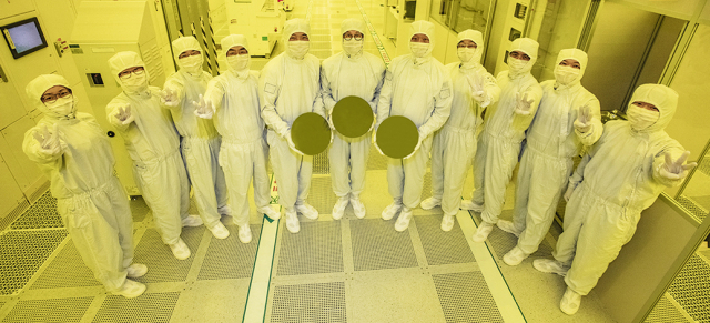 Samsung Electronics announced on the 30th that it has started the initial mass production based on the world's first 3-nanometer foundry process applying GAA (Gate-All-Around) technology. The photo shows key figures from the Foundry Business Division, Semiconductor Research Center, and Global Manufacturing & Infrastructure who participated in the 3-nanometer foundry mass production posing for a commemorative photo. / Photo by Yonhap News
During Samsung's '7nm gap,' TSMC aggressively captured cutting-edge system semiconductor orders from other design companies and grew rapidly. After receiving EUV equipment from ASML, TSMC produced '7nm+' semiconductors with much more stabilized quality.
Thanks to EUV, which enabled much more precise circuit work than previous patterning processes, both companies smoothly reached 5nm and 4nm processes, but the gap that once opened was not easily closed. According to global market research firm TrendForce, in the first quarter of this year, TSMC recorded a 53.6% share of the global foundry market, while Samsung held 16.3%, ranking second. The gap between the two companies widened by 3.5 percentage points compared to the previous quarter.
◆Samsung begins 3nm mass production, will it counterattack TSMC?
Just as the two companies have been neck and neck for 15 years, technological superiority can be overturned at any time. Samsung announced on the 30th that it has started the world's first mass production of 3nm semiconductors. This is up to six months ahead of TSMC, which plans to begin 3nm semiconductor production in the second half of this year.
Technologically, Samsung's 3nm is known to be more advanced than TSMC's 3nm. Samsung applied a new type of transistor using the Gate All Around (GAA) structure to improve data processing speed and power efficiency. In contrast, TSMC's 3nm semiconductors, scheduled for production at the end of this year, will continue to use the existing FinFET transistor structure. Samsung's start of 3nm mass production is attracting attention as a potential 'beginning of a counterattack' to narrow the market share gap with TSMC.
© The Asia Business Daily(www.asiae.co.kr). All rights reserved.


