For Developing New Technologies and Leading the Market in Future Strategic Business Areas
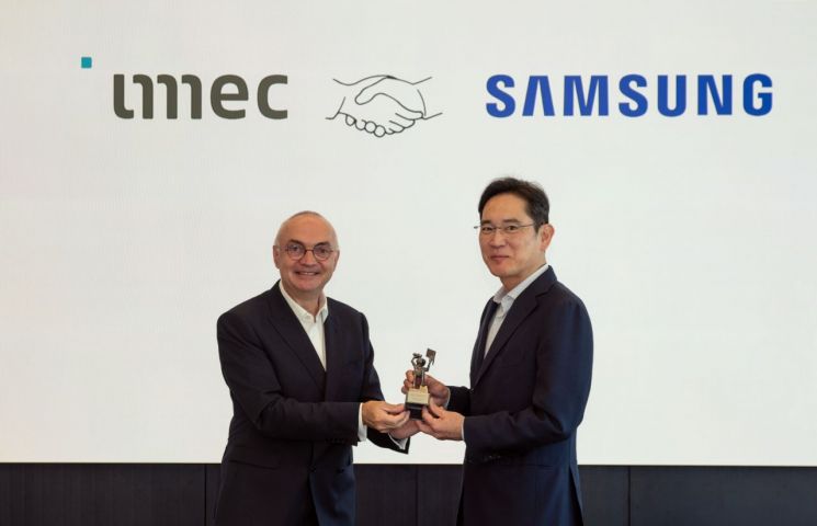 Samsung Electronics Vice Chairman Lee Jae-yong visited imec located in Leuven, Belgium on the 15th (local time) and took a commemorative photo with imec CEO Luc Van den Hove.
[Asia Economy Reporter Park Sun-mi] Samsung Electronics Vice Chairman Lee Jae-yong's visit to imec, Europe's largest comprehensive semiconductor research institute, during his business trip to Europe is interpreted as a move to concretize the plan to invest 450 trillion won over the next five years focusing on future new businesses.
On the 16th, Samsung Electronics announced that Vice Chairman Lee visited imec, Europe's largest comprehensive semiconductor research institute located in Leuven, Belgium, on the 15th (local time) and met with CEO Luc Van den Hove to discuss the latest technologies and research and development directions in the semiconductor field. imec is Europe's largest comprehensive semiconductor research institute jointly established in 1984 by Belgium, France, and the Netherlands. It partners with semiconductor companies worldwide, including Samsung Electronics, to research and develop advanced technologies.
However, imec's research areas are not limited to semiconductor design, process technology, materials, and equipment. It also conducts advanced research in various cutting-edge fields such as artificial intelligence (AI), life sciences, and future energy. Recognized as a research and development hub for nanotechnology and digital technology, imec currently has over 4,500 researchers from 95 countries conducting multinational research beyond national borders, focusing on future technologies expected to be commercialized in 3 to 10 years.
Vice Chairman Lee, who visited imec, was confirmed to have received introductions to advanced research projects underway at imec, including ▲AI ▲bio and life sciences ▲future energy, in addition to state-of-the-art semiconductor process technologies, and inspected the research and development site. This visit can be interpreted as an effort to develop new technologies and lead the market in future strategic business areas.
Last month, Samsung announced its 'Preparing for Samsung's Future' plan, stating it will invest 450 trillion won over the next five years focusing on future new businesses such as semiconductors, bio, and new growth IT (AI and next-generation communications). An industry insider explained, "Since imec conducts advanced research in various fields including semiconductors, ▲AI ▲life sciences and bio ▲future energy, it aligns with Samsung's future strategic business areas such as semiconductors, bio, and new growth IT."
Meanwhile, just before visiting Belgium, Vice Chairman Lee visited the ASML headquarters located in Eindhoven, the Netherlands, and met with CEO Peter Wennink to discuss ways to strengthen cooperation between the two companies. They broadly discussed future semiconductor technology trends, semiconductor market outlook, smooth supply of EUV lithography equipment essential for implementing fine processes for next-generation semiconductor production, and mid- to long-term business directions for both companies. This was Vice Chairman Lee's first visit to ASML headquarters in the Netherlands in 20 months since October 2020. Samsung Electronics DS Division head Kyung Kye-hyun was also confirmed to have attended the meeting.
© The Asia Business Daily(www.asiae.co.kr). All rights reserved.

![Clutching a Stolen Dior Bag, Saying "I Hate Being Poor but Real"... The Grotesque Con of a "Human Knockoff" [Slate]](https://cwcontent.asiae.co.kr/asiaresize/183/2026021902243444107_1771435474.jpg)


