Both Leaders Tour Manufacturing Facility for Over 20 Minutes
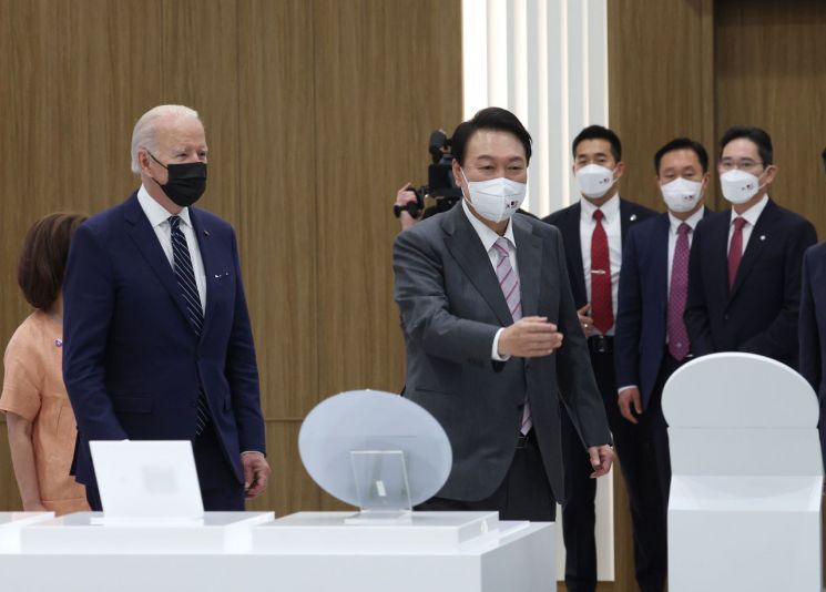
[Asia Economy Reporter Ki-min Lee] On the 20th, President Yoon Suk-yeol met U.S. President Joe Biden, who arrived in Korea, for the first time at Samsung Electronics' Pyeongtaek semiconductor campus and toured the factory together.
President Biden arrived at Osan Air Base in Gyeonggi Province at around 5:22 p.m. that day. After disembarking from Air Force One, the presidential aircraft, President Biden removed his sunglasses and mask and greeted Foreign Minister Park Jin, who was waiting for him.
At around 6:11 p.m., as his first schedule in Korea, President Biden arrived at Samsung Electronics' Pyeongtaek campus and met President Yoon, who was waiting, exchanging a handshake as their first greeting. The two leaders exchanged brief greetings, and President Biden lightly tapped President Yoon on the shoulder, creating a relaxed atmosphere.
The event held at the Samsung semiconductor campus that day was attended on the Korean side by Foreign Minister Park Jin, Minister of Trade, Industry and Energy Lee Chang-yang, Minister of Science and Technology Lee Jong-ho, National Security Office Chief Kim Sung-han, and Chief Secretary for Economic Affairs Choi Sang-mok. The U.S. side was represented by Commerce Secretary Gina Raimondo, National Security Advisor Jake Sullivan, and White House Deputy Chief of Staff Jen Dillon.
After commemorative photos and informal talks, Presidents Yoon and Biden listened to an explanation of the 3-nanometer wafer prototype, which incorporates Samsung Electronics' latest semiconductor manufacturing technology. The prototype explanation was given by Samsung Electronics Vice Chairman Lee Byung-hoon.
The two leaders toured the semiconductor manufacturing facilities from 6:56 p.m. to 7:18 p.m. under the accompaniment of Samsung Electronics Vice Chairman Lee Jae-yong. Presidents Yoon and Biden observed for more than 10 minutes each the manufacturing facilities at P1, which produces memory semiconductors, and P3, currently under construction, at the Pyeongtaek campus.
Vice Chairman Lee introduced the Pyeongtaek campus facilities and technology status to the two leaders and reportedly answered their questions. Samsung Electronics' Pyeongtaek campus is the world's largest state-of-the-art semiconductor production base, and the P3 under construction is the world's largest manufacturing plant (Fab).
President Biden's visit to Samsung Electronics' semiconductor campus as his first schedule in Korea and his direct inspection of the manufacturing facilities are seen as the start of global supply chain cooperation and economic security based on the Korea-U.S. technological alliance. The two leaders are expected to express their commitment to strengthening the Korea-U.S. economic security alliance through semiconductors while touring the factory together.
A presidential office official emphasized, "Until now, the Korea-U.S. alliance has been discussed only in terms of military and security alliances, but now is the time when comprehensive cooperation begins," adding, "Since the first schedule was set at the semiconductor site, which is deeply related to both countries' interests, it will be an opportunity to promote the Korea-U.S. technological alliance in the global market."
Jake Sullivan, U.S. White House National Security Advisor, also explained the purpose of visiting the Pyeongtaek semiconductor plant during a briefing on the plane, stating, "What President Biden wants to strengthen is the advanced technology ecosystem between democracies and free societies that must be protected from predation by other countries."
© The Asia Business Daily(www.asiae.co.kr). All rights reserved.


