Designed with proprietary patented technology
Durability extended from 1 week to 1 year
Tested by US semiconductor equipment company
Sensitivity twice as high as competitors
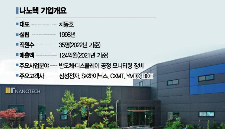
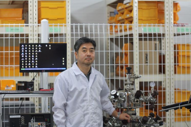
[Asia Economy Reporter Kwak Minjae] The 'Plasma Process Monitoring Equipment' is a core component in the semiconductor front-end process. The processes of etching (cutting) or deposition (stacking thin films) of semiconductor raw material wafers take place in a vacuum environment. If impurities or air enter during this process, it causes significant problems. Plasma process monitoring equipment is a sensor that monitors process changes in real-time to detect impurities. If an accident occurs once during the semiconductor process, an average of 75 wafers become unusable, resulting in a loss of 2 to 3 billion KRW at the fab (factory). If defects are not detected in advance, a huge amount of time and money is invested in semiconductors with no commercial value, making the scale of loss even greater. This is why the role of plasma process monitoring equipment is so important. NanoTech CEO Cha Dongho, a semiconductor and display monitoring process equipment company, said, "NanoTech has localized the SPOES sensor by combining plasma generation technology and spectrum analysis technology," adding, "Based on overwhelming technological prowess, we currently hold a 90% domestic market share and over 70% global market share in the SPOES sensor sector, ranking first worldwide."
CEO Cha Dongho: "10% of sales revenue
invested in R&D and dedicated to technology development
The importance of real-time process monitoring technology
will continue to grow"
Outstanding durability and sensitivity... Number one in global market share
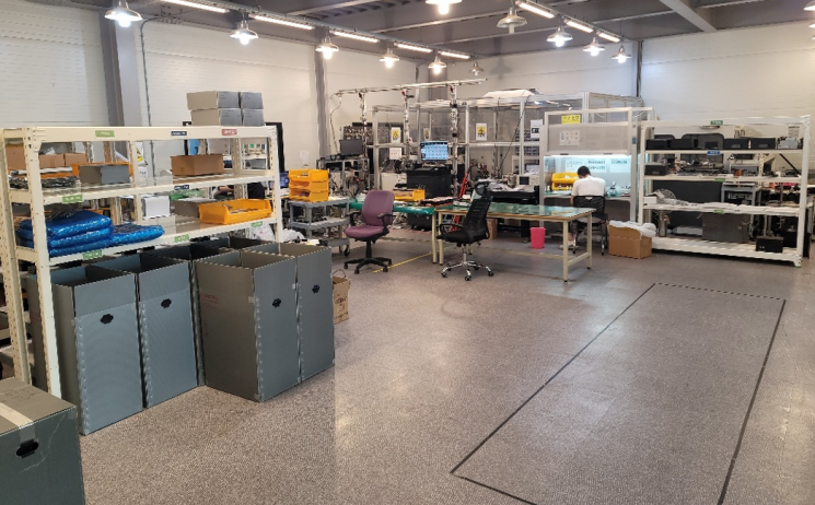
NanoTech specializes in plasma process monitoring equipment. The SPOES (Self Plasma OES; OES = Optical Emission Spectroscopy) sensor emits plasma light into gases discharged through the exhaust line of semiconductor manufacturing equipment and analyzes wavelengths from 200 nm (nanometers, one-billionth of a meter) to 850 nm via a spectrometer to detect impurities and air intrusion in a vacuum environment. Since vacuum processes are similar in semiconductor and display manufacturing, this product is also used in display processes. Major clients include Samsung Electronics, SK Hynix, and China's Changxin Memory (CXMT) and Yangtze Memory (YMTC). BOE, China's largest display manufacturer (which grew explosively after acquiring Hyundai Electronics' LCD division in 2003, now Hynix), also uses NanoTech products.
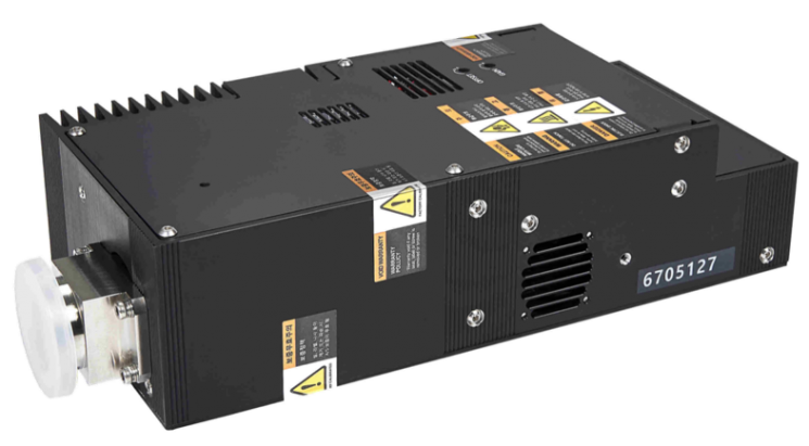
The SPOES sensor, designed with NanoTech's proprietary patented technology, boasts several months longer durability and twice the sensitivity compared to competitors' products. Existing products were vulnerable to contamination due to continuous exposure to gases inherent to sensor characteristics. Severe contamination could cause the plasma to extinguish, preventing real-time monitoring. However, NanoTech extended the SPOES sensor's durability from one week to one year using patented technology that minimizes contamination. In past impurity sensitivity tests conducted by a U.S. semiconductor equipment company, NanoTech's sensor demonstrated performance twice as good as competitors. CEO Cha said, "By investing 10% of annual sales revenue into research and development (R&D) and dedicating ourselves to technology development, we have become the company with the most outstanding technology in this field," adding, "As semiconductor nano processes advance and become sensitive even to minute impurities, the importance of real-time process monitoring technology will continue to grow."
Supplies to Samsung, SK Hynix,
as well as China's Changxin Memory and BOE
Plans to establish subsidiaries in the U.S. and Japan
Aiming to become a global equipment company
Currently, the sales ratio is approximately 60% domestic and 40% export. Last year, the company recorded 12.4 billion KRW in sales and 6 billion KRW in operating profit. Sales increased by 90% and operating profit by 225% compared to the previous year, marking a flourishing period for the 25-year-old company amid the semiconductor market boom. China's concentrated investment in display and semiconductor sectors has been a boon. CEO Cha explained, "China's focused investment to catch up with Samsung and LG in display and semiconductor sectors has caused explosive growth in demand for our products."
From repairing semiconductor measuring instruments to partnership with Samsung Electronics
CEO Cha founded Alteck, the predecessor of NanoTech, in 1998. He decided to start the business after the company he previously worked for faced financial difficulties. Initially, he began by repairing semiconductor measuring instruments at semiconductor research institutes. Seeing products discarded due to irreparable damage motivated him to localize plasma process monitoring equipment. In 2006, NanoTech showcased the newly developed SPOES sensor at a semiconductor exhibition, which became the opportunity to supply Samsung Electronics. At that time, Samsung Electronics was seeking monitoring equipment for the semiconductor deposition process, and NanoTech's product caught the attention of Samsung Electronics researchers. CEO Cha said, "This opportunity allowed us to test the SPOES sensor for supply to Samsung Electronics," adding, "After two years of testing and competition with five companies from the U.S., France, and others, we were finally selected due to superior durability and sensitivity."
NanoTech plans to establish overseas subsidiaries in the U.S. and Japan to become a global comprehensive monitoring equipment company. Although it currently holds the global number one position in the SPOES sensor sector, targeting the U.S. and Japanese markets?home to three of the world's top semiconductor equipment companies?is crucial to becoming a global comprehensive monitoring equipment company. To strengthen technology, NanoTech began developing ICP-MASS sensors two years ago. While existing sensors detect impurities down to 25 PPM (parts per million), the newly launched sensors will detect below 1 PPM. As Samsung Electronics accelerates investment in 3 nm foundry processes to catch up with Taiwan's TSMC, demand for NanoTech's new products is expected to increase accordingly.
© The Asia Business Daily(www.asiae.co.kr). All rights reserved.


