Energy Technology Research Institute and Chungbuk National University Develop Innovative Technology for Silicon Wafer Manufacturing Process
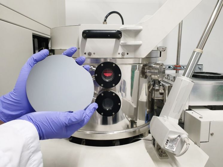 The plasma epitaxial silicon with maximized interfacial porosity jointly developed by the Korea Institute of Energy Research and Chungbuk National University.
[Asia Economy Reporter Kim Bong-su] Domestic researchers have developed an innovative technology to manufacture single-crystal silicon wafers, a core material for silicon solar cells and semiconductor devices, without wasting raw materials through a reverse thinking approach. This technology is attracting attention as it can reduce manufacturing costs by up to half.
The Korea Institute of Energy Research, in collaboration with Chungbuk National University, announced on the 11th that they have developed a technology to easily peel off silicon wafers by growing single-crystal silicon upward on a mother substrate and then utilizing plasma epitaxial silicon, which was previously considered defective due to its porous structure, in reverse?similar to peeling along a perforation line.
The results of this research were published as a cover paper on the 14th of last month in the international materials science journal Advanced Materials (IF 30.849).
The core of this technology is to control the porous structure of plasma epitaxial silicon and peel off the entire single-crystal silicon wafer grown on top, thereby innovating the manufacturing process. The conventional method for producing epitaxial silicon wafers forms a porous silicon separation layer downward on the upper part of the mother substrate, grows single-crystal silicon, and then separates it by peeling. However, this method causes partial detachment of the mother substrate surface, leading to gradual loss of the mother substrate and increased manufacturing costs after multiple peeling processes.
Research on plasma epitaxial silicon has been conducted since the mid-2000s, but due to its high defect density and porous characteristics, it was treated as a defect occurring during solar cell processes. Most studies focused on suppressing the growth of this material or reducing defects and porosity within it.
Instead, the research team applied reverse thinking to plasma epitaxy by intentionally increasing defect density and maximizing interface porosity. In other words, just as bubbles in bread dough make it soft, they used defects and holes during silicon wafer production to weaken the parts to be peeled off.
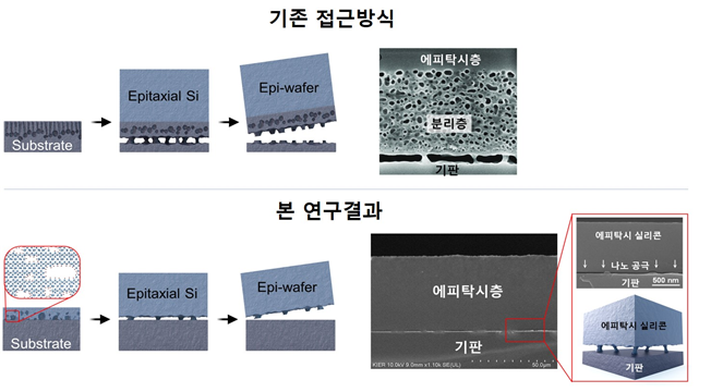
The research team grew porous plasma epitaxial silicon on a mother substrate, then created a thin, easily detachable gap through a heat treatment process. Afterward, when crystalline silicon is thickly deposited on top, the wafer usable for solar cells or other semiconductor devices can be easily separated along the perforation line, and the mother substrate can be reused infinitely without damage.
They also discovered for the first time the phenomenon of nano-gap formation caused by the reconstruction of the nano-porous structure and pores of plasma epitaxial silicon grown by chemical vapor deposition, and identified its cause. They confirmed that, similar to nano-sized pores inside materials bonding at high temperatures, the same phenomenon occurs in solids under a high-temperature hydrogen environment. By controlling the nano-porous structure where pores merge and move to the surface to disappear, only a few pillars supporting the silicon grown on top remain, creating a structure that is easy to peel off.
This drastically reduces raw material waste and cuts solar cell manufacturing costs in half. Moreover, since it is based on chemical vapor deposition, widely used for plasma epitaxial silicon and single-crystal silicon growth, it is expected to have significant industrial impact by being applicable to various next-generation semiconductor devices.
Professor Kim Ga-hyun of Chungbuk National University said, “Plasma epitaxial silicon has been treated only as a defect occurring during high-efficiency solar cell processes, but our reverse thinking approach to maximize porosity has pioneered a new research field. As the beginning of research on this new material, we will continue studying the nano-porous structure of plasma epitaxial silicon and explore applicable fields using this material.”
© The Asia Business Daily(www.asiae.co.kr). All rights reserved.


