2.5D 'H-Cube'... Equipped with More Than Six High-Bandwidth Memory HBM
Customized Packages for AI, Data Centers, 5G, and Other Applications
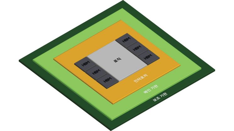 Samsung Electronics Next-Generation 2.5D Packaging Solution 'H-Cube' Configuration Diagram
[Photo by Samsung Electronics]
[Asia Economy Reporter Kim Heung-soon] Samsung Electronics announced on the 11th that it has developed a high-performance semiconductor 2.5D packaging solution called ‘H-Cube (Hybrid-Substrate Cube)’ needed for artificial intelligence (AI), data centers, 5G, and autonomous driving.
Packaging is a technology that connects different types of semiconductors with unique performances, such as DRAM, NAND, and logic, vertically or horizontally to create a single semiconductor, and it is called a post-process in semiconductor manufacturing.
As technology advances and the amount of data to be processed increases, the types and numbers of semiconductors installed in finished products (sets) increase. If these are individually attached to substrates, the overall size of the set increases and development costs inevitably rise. For this reason, advanced packaging technology that connects different types into a single semiconductor has become a core competitive advantage in the semiconductor industry.
The newly developed H-Cube by Samsung Electronics is a 2.5D packaging solution that can mount six or more High Bandwidth Memory (HBM) chips on a silicon fine circuit substrate (interposer). 2.5D packaging is a technology that vertically connects chips through Through Silicon Vias (TSV).
Samsung Electronics explained, "Using this technology, it is possible to achieve much higher density connectivity compared to connecting chips through conventional PCBs (printed circuit boards)," adding, "It can be used for high-spec semiconductors such as AI semiconductors and HPC (high-performance computing)."
Samsung Electronics narrowed the spacing of 'solder balls' that electrically connect the main substrate and auxiliary substrate by 35% compared to the existing standard to minimize the size of the substrate, and technically solved the difficulty of manufacturing large-area substrates caused by mounting multiple HBMs.
H-Cube was developed through collaboration between Samsung Electronics, Samsung Electro-Mechanics, and Amkor Technology, a semiconductor packaging specialist. Kang Moon-soo, Executive Vice President of the Market Strategy Team at Samsung Electronics’ Foundry Business Division, said, "As a result of long-term cooperation with these companies, we have completed the optimal solution for high-spec semiconductors that require integration of many chips," adding, "We will continue to provide customized semiconductors tailored to customer demands in various package forms for application-specific markets such as data centers, AI, and networks through close cooperation with foundry partners."
Kim Jin-young, Senior Vice President of Amkor Technology’s Technical Research Institute, said, "By successfully developing the H-Cube solution with Samsung Electronics, we have overcome the challenges of semiconductor integration technology required in the HPC and AI markets," and evaluated, "It is highly meaningful that a successful collaboration relationship between foundries and OSAT (Outsourced Semiconductor Assembly and Test) companies has been established."
Meanwhile, Samsung Electronics’ Foundry Business Division received the Presidential Citation for National Quality Management at the ‘47th National Quality Management Convention’ held on the 8th. This is the first time that Samsung Electronics’ semiconductor division has received the Presidential Citation for National Quality Management. Samsung Electronics will hold the ‘3rd SAFE (Samsung Advanced Foundry Ecosystem) Forum’ online on the 18th to strengthen the foundry ecosystem.
© The Asia Business Daily(www.asiae.co.kr). All rights reserved.


