Samsung Electronics-Harvard Joint Research Published in Nature Electronics
Proposed Technology to Copy and Paste Brain Neural Network Connection Maps onto Memory Chips
Presented Vision for Next-Generation AI Semiconductors Reproducing Brain's Unique Functions
[Asia Economy Reporter Suyeon Woo] Samsung Electronics and researchers from Harvard University in the United States have presented a future vision for next-generation artificial intelligence semiconductor technology called Neuromorphic chips.
On the 26th, Samsung Electronics announced that a paper authored by Donhee Ham, Fellow at Samsung Electronics’ Advanced Institute of Technology and professor at Harvard University, Hongkeun Park, professor at Harvard University, Sungwoo Hwang, President of Samsung SDS, and Kinam Kim, Vice Chairman of Samsung Electronics, was published on the 23rd local time in the world-renowned academic journal Nature Electronics.
This paper proposed a technological vision for neuromorphic chips that reproduce the brain’s intrinsic functions by ultra-high-sensitivity measurement of electrical signals of neurons in brain neural networks using nanoelectrodes to “copy” the connection map between neurons and “paste” the copied map onto memory semiconductors.
Neuromorphic semiconductors are semiconductors inspired by or directly mimicking the human brain neural network, with the ultimate development goal of reproducing high-level brain functions such as cognition and reasoning.
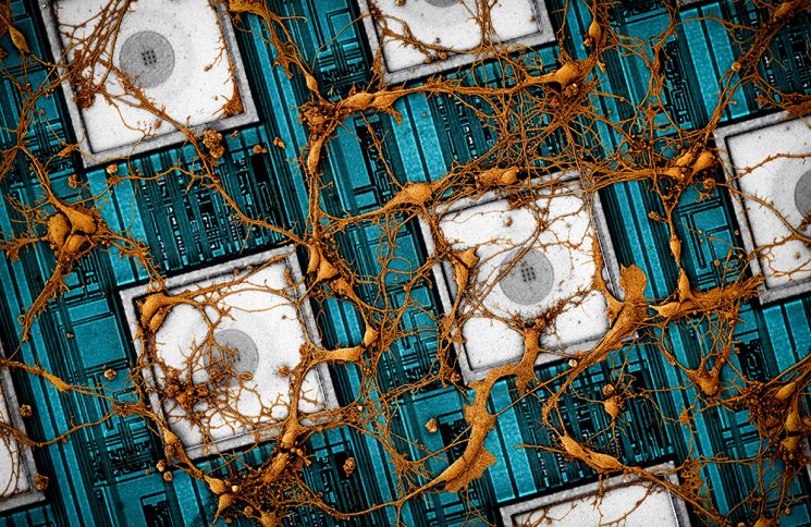
The “copying” of neural network maps through ultra-high-sensitivity measurement is achieved by the arrangement of nanoelectrodes penetrating the neurons. By penetrating inside the neurons, the measurement sensitivity increases, allowing the detection of faint electrical signals occurring at the synapses between neurons. This enables the identification of those synapses and the mapping of the neural network. Samsung Electronics has been continuously collaborating with the Harvard research team on developing this technology since 2019.
In particular, Samsung Electronics proposed a completely new concept of neuromorphic semiconductors where the copied neural network map is “pasted” onto memory semiconductors, with each memory cell acting as a synapse between neurons. Additionally, since analyzing the vast amount of signals measured from the neural network on a computer to construct the neural network map takes a lot of time, they presented a groundbreaking technical perspective to directly drive the memory platform with the measured signals to quickly download the neural network map. This platform can utilize commonly used memories such as flash and other forms of non-volatile memories like resistive RAM (RRAM).
Meanwhile, to ultimately implement about 100 trillion synapses in the human brain as a memory network, memory integration density must be maximized. To this end, they proposed the use of cutting-edge semiconductor technologies such as 3D flash stacking technology and 3D packaging through TSV (Through Silicon Via), which is applied to high-performance DRAM.
This research is also significant in that technology leaders from academia and industry participated to combine neuroscience and memory technology, showing a vision for next-generation artificial intelligence semiconductors. Samsung Electronics plans to continue focusing on neuromorphic research based on its existing semiconductor technology capabilities to secure technological leadership in the next-generation artificial intelligence semiconductor field.
Fellow Ham said, “The bold approach proposed in this paper will broaden the boundaries of memory and system semiconductor technologies and help further advance neuromorphic technology.”
© The Asia Business Daily(www.asiae.co.kr). All rights reserved.


