[Asia Economy Reporter Kim Hyewon] SK Hynix is making its first foray into mass production of next-generation DRAM using extreme ultraviolet (EUV) processes. Amid growing expectations for a semiconductor market super cycle (long-term boom), with DRAM prices rebounding for the first time in eight months since early this year, the company has built the largest semiconductor factory equipped with state-of-the-art EUV equipment and launched a competition for supremacy in advanced process technology.
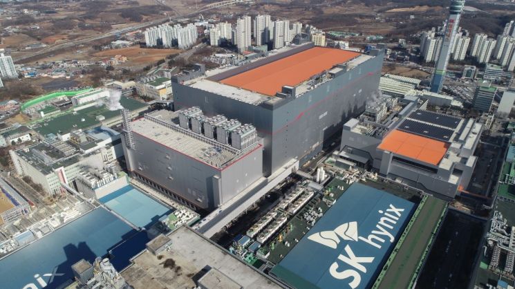
On the 1st, SK Hynix held a completion ceremony for its semiconductor factory M16 at its headquarters in Icheon, Gyeonggi Province. To comply with COVID-19 prevention guidelines, the ceremony was held simply, attended by 16 people including SK Group Chairman Chey Tae-won, SK Group Senior Vice Chairman Chey Jae-won, SK Supex Council Chairman Cho Dae-sik, SK Hynix Vice Chairman Park Jung-ho, and SK Hynix CEO Lee Seok-hee. Employees and partner company staff joined remotely via video conference.
Chairman Chey said, "Two years ago, when the semiconductor market was in decline and we announced plans to build M16, there were many concerns. But now that talks of a semiconductor upcycle are emerging, the bold decision made during difficult times has allowed us to dream of a greater future." He added, "M16 is the completion of the grand plan the company has envisioned so far and will remain an important symbol as the starting point leading to the Yongin cluster."
Construction of M16 began in November 2018 and was completed in 25 months, with a total construction cost of 3.5 trillion won and a total workforce of 3.34 million person-days. The building area covers 57,000㎡ (about 17,000 pyeong), equivalent to eight soccer fields, with dimensions of 336m in length, 163m in width, and a height of 105m, equivalent to a 37-story apartment. It is the largest production facility SK Hynix owns domestically and internationally.
Notably, M16 is significant as the first factory equipped with EUV equipment for next-generation DRAM mass production. It is the first time SK Hynix has introduced EUV lithography equipment. Starting in the second half of this year, SK Hynix plans to produce 4th generation 10-nanometer class (1a) DRAM products using EUV equipment. The full-scale application of the EUV process is set for 5th generation DRAM. SK Hynix CFO Noh Jong-won explained, "Most fabs have multi-layer structures, but M16 is the world's largest fab with a three-layer structure. We will flexibly adjust mass production plans to meet market demand while monitoring the DRAM market situation through the end of the year." On the same day, SK Hynix held an event to remotely present plaques of merit and appreciation to those who contributed to the construction of M16 and key partners.
Meanwhile, Chairman Chey was unanimously nominated as the next chairman at the regular meeting of the Seoul Chamber of Commerce and Industry’s chairman group. If he is officially elected as chairman of the Seoul Chamber at the extraordinary general meeting on the 23rd of next month, he will serve a three-year term. Typically, the chairman of the Seoul Chamber also serves as chairman of the Korea Chamber of Commerce and Industry. Chairman Chey is the first head of a top four domestic conglomerate to hold the position of chairman of the Korea Chamber.
© The Asia Business Daily(www.asiae.co.kr). All rights reserved.


