[Asia Economy Reporter Ki-min Lee] Samsung Electronics has taken a step closer to the 'future semiconductor' by discovering a new material that can make semiconductors smaller and faster, as well as applicable to existing processes.
According to Samsung Electronics on the 6th, Samsung Advanced Institute of Technology recently succeeded in discovering a new material called amorphous boron nitride (a-BN) in collaboration with Ulsan National Institute of Science and Technology (UNIST). This is a significant discovery of a new material 16 years after the University of Manchester research team in the UK discovered graphene, known as the 'dream material.' The research results of Samsung Electronics and UNIST were also introduced last month in the world-renowned British academic journal Nature.
So far, the semiconductor industry has increased the integration density per unit area to improve device performance. The higher the integration density, the more information can be processed quickly in a smaller size. However, as integration density increases, technical problems such as loss of information storage capability or electrical interference between circuits occur.
For this reason, 2D materials are regarded as the key to solving the semiconductor industry's challenges. 2D materials exhibit strong properties of conductors, insulators, or semiconductors even at the atomic level, the smallest unit of matter, and are very thin?about one hundred-thousandth the thickness of an A4 sheet of paper (approximately 0.1 mm)?making them flexible yet strong. Among 2D materials, graphene is the most representative. Samsung Advanced Institute of Technology has researched and developed core technologies to produce large-area graphene and apply it to semiconductor processes for several years. Based on these core technologies, they have recently focused on applying graphene to wiring, the electrical paths along semiconductor circuits, because graphene’s dense hexagonal structure acts as a thin and strong barrier that reduces resistance.
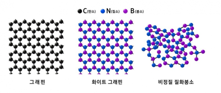
The research team not only secured a world-class low dielectric constant of 1.78 but also demonstrated that the material can grow over a large area on semiconductor substrates even in low-temperature (400℃) environments. The dielectric constant measures the efficiency of electric charge accumulation on the material’s surface; the lower the value, the lower the electric flow and thus reduced electrical interference. The dielectric constant of currently used porous organosilicates is around 2.5 to 2.7. Amorphous boron nitride can be applied across memory semiconductors (such as DRAM and NAND) as well as system semiconductors. Its use is especially anticipated in high-performance server memory semiconductors.
Samsung Advanced Institute of Technology plans to continue efforts to develop next-generation materials by establishing technical collaborations with domestic and international universities. Seong-jun Park, Executive Director leading 2D material research and development at Samsung Advanced Institute of Technology, said, "Although the development of 2D materials and derived new materials is accelerating recently, additional research and development by academia and industry are necessary for immediate application to processes. We will continue to strive not only in new material research and development but also in enhancing process applicability to lead the paradigm shift in semiconductors."
© The Asia Business Daily(www.asiae.co.kr). All rights reserved.


