Ministry of Science and ICT Future Materials Discovery Project and Samsung Future Technology Development Project Support This Research
Domestic Research Team's Sole Corresponding Study Published in World-Renowned Journal 'Science'
Discovery of Physical Phenomenon Offsetting Interatomic Elastic Interactions Applied to Semiconductors
Memory Semiconductor Miniaturization Possible Down to 0.5 nm from Existing 10 nm
[Asia Economy Reporter Ki-min Lee] A research team led by Professor Junhee Lee of the Department of Energy and Chemical Engineering at Ulsan National Institute of Science and Technology (UNIST), supported by the Samsung Future Technology Development Project, has announced a theory and material that can improve the integration density of next-generation memory semiconductors by more than 1,000 times.
Samsung Electronics announced on the 3rd that this research was published on the 2nd (local time) in the world-renowned American scientific journal 'Science.' It is rare for a purely theoretical paper to be published in Science. This research, conducted solely by a domestic research team as the corresponding author, was recognized for its theoretical rigor, originality, and industrial impact.
The semiconductor industry has been increasing integration density per unit area by miniaturizing devices to improve performance. However, for data storage, 'domains'?clusters of thousands of atoms connected elastically?are essential, and their size could not be reduced below a certain level. When semiconductor devices shrink below this limit, a 'scaling' issue occurs, causing the loss of the ability to store information. When the scaling issue arises, the fundamental operation of semiconductors, representing 0 and 1, cannot be properly implemented.
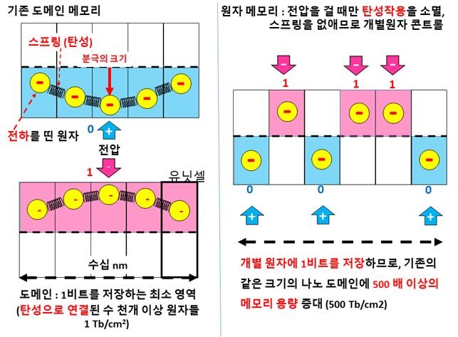 Comparison between memory storing data in single atoms proposed by the research team (right) and memory storing data using domains consisting of thousands of atoms (left). Conventional memory stores 1 bit using domains of tens of nanometers in size due to elastic interactions between atoms, but by utilizing the phenomenon proposed by the research team, the elastic interactions between atoms disappear when voltage is applied, enabling data storage in individual atoms.
 Comparison of memory storing data in a single atom proposed by the research team (above) and memory storing data using domains consisting of thousands of atoms (below). Existing memory stores 1 bit using domains of tens of nanometers in size due to elastic interactions between atoms, but
by utilizing the phenomenon proposed by the research team, the elastic interaction between atoms disappears when voltage is applied, enabling data storage in individual atoms.
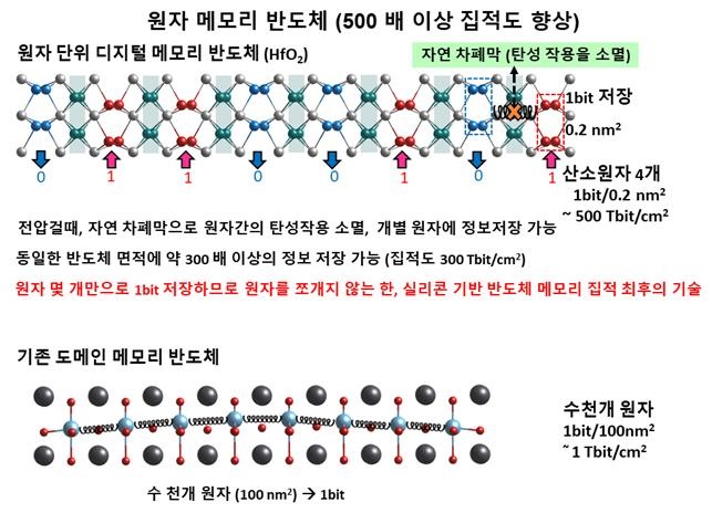
Professor Lee's research team discovered a new physical phenomenon in the semiconductor material 'hafnium oxide (HfO2),' where applying voltage to oxygen atoms eliminates atomic elasticity, and successfully applied this to semiconductors to overcome storage capacity limits.
By applying this phenomenon, individual atoms can be controlled, enabling data storage (1 bit) in four oxygen atoms, eliminating the need for domains sized in tens of nanometers.
Hafnium oxide is a commonly used material in current memory semiconductor processes, and applying this phenomenon is expected to significantly enhance memory performance in various products such as smartphones and tablets.
In particular, the research team noted that applying these results prevents the loss of storage capacity when semiconductors are miniaturized, allowing semiconductor processes currently halted at about 10 nm to be further miniaturized to 0.5 nm. Accordingly, the research team expects memory integration density to improve by approximately 1,000 times compared to existing levels.
Professor Lee said, "Technology that stores information in individual atoms is the ultimate integration technology within the limits of not splitting atoms," adding, "We expect this technology to accelerate semiconductor miniaturization even further."
This research was selected as a project under the Samsung Future Technology Development Project in December last year and has been supported by the Ministry of Science and ICT's Future Materials Discovery Project.
Meanwhile, the Samsung Future Technology Development Project plans to support national future science and technology research with 1.5 trillion KRW over 10 years since 2013, and has so far allocated 758.9 billion KRW in research funds to 589 projects.
Under Samsung Electronics' CSR vision 'Together for Tomorrow! Enabling People,' the company is conducting win-win activities and youth education social contribution activities, including the Samsung Future Technology Development Project, smart factories, C-Lab Outside, and the partner company win-win fund.
 Junhee Lee, Professor, Department of Energy and Chemical Engineering, Ulsan National Institute of Science and Technology (UNIST)
© The Asia Business Daily(www.asiae.co.kr). All rights reserved.
![Clutching a Stolen Dior Bag, Saying "I Hate Being Poor but Real"... The Grotesque Con of a "Human Knockoff" [Slate]](https://cwcontent.asiae.co.kr/asiaresize/183/2026021902243444107_1771435474.jpg)


