[Asia Economy Reporter Junho Hwang] A domestic research team has elucidated the optical phenomena of irregularly arranged high-density nanowire bundles and developed a large-area fabrication technology. This technology is expected to be applied in developing artificial retinas with resolution better than the human eye, lightweight flexible solar cells, and physically unclonable hardware. On the 18th, Professor Youngmin Song's research team from the Department of Electrical, Electronics and Computer Engineering at Gwangju Institute of Science and Technology announced that their research results were introduced in the international journal Advanced Optical Materials.
The research team elucidated the microscopic optical phenomena occurring within high-density, irregular semiconductor nanowire bundles?previously overlooked?through a 3D wave equation-based analytical method and experimentally verified the findings.
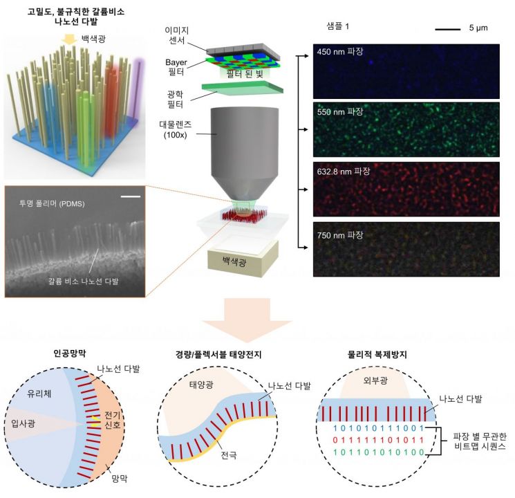
A nanowire bundle is a cluster made by bundling multiple nanowires, each with a thickness one-thousandth that of a human hair. Vertical semiconductor nanowires (arrays) based on semiconductor materials possess excellent mechanical, electrical, and optical properties, making them promising materials for next-generation electronic devices. Semiconductor nanowire arrays have mainly been studied for applications in devices such as high-efficiency solar cells, image sensors, and lasers because they produce optical spectral phenomena observable in the macroscopic world.

Additionally, the research team developed a technology to fabricate optimal nanowire bundles. They grew high-density, extremely thin gallium arsenide nanowire bundles on the entire surface of a silicon wafer. Then, by coating the grown nanowire bundles with a transparent polymer called PDMS and scraping them off with a razor blade, they separated the high-density nanowire bundles.
The research team stated that by applying this method, nanowire bundles can be grown on inexpensive silicon wafers, and after separating the grown nanowire bundles, the wafer can be reused, making the process very economical.
Professor Youngmin Song said, "The greatest significance of this research lies in elucidating the microscopic optical phenomena within nanowire bundles, which had not been previously illuminated, and overcoming the limitation of existing vertical semiconductor nanowire arrays that require electron beam lithography processes." He added, "In particular, the selective wavelength absorption characteristics of nanowire bundles can be used as physically unclonable security hardware and are expected to be used as artificial retina materials with resolution much higher than the human eye."
© The Asia Business Daily(www.asiae.co.kr). All rights reserved.
![Clutching a Stolen Dior Bag, Saying "I Hate Being Poor but Real"... The Grotesque Con of a "Human Knockoff" [Slate]](https://cwcontent.asiae.co.kr/asiaresize/183/2026021902243444107_1771435474.jpg)


