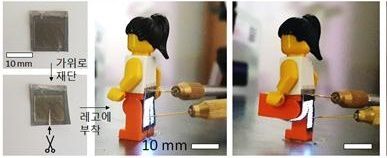
 The research team cut LED panels with scissors to fit the shape of Lego minifigure legs and attached them to study LED illumination in various poses.
[Asia Economy Reporter Junho Hwang] A technology for LED panels that can be bent, folded, and cut with scissors has been developed. It is expected to provide a new clue for the development of wearable displays that can be attached to curved surfaces, human bodies, or robot joints. The National Research Foundation of Korea announced on the 4th that the joint research results of Sejong University and the University of Texas research teams, containing these findings, were published in the international academic journal Science Advances.
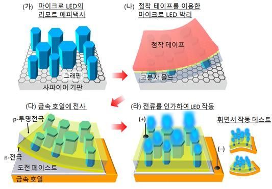
The research team developed gallium nitride micro LEDs that can be easily detached from the substrate and freely reshaped. The LED panel was composed by implanting tens of thousands of nanoscale single-crystal micro LEDs on a graphene-coated single-crystal sapphire substrate.
Because the graphene does not come into direct contact with the LEDs, it can be easily separated from the substrate. It can be peeled off as easily as with adhesive tape. Also, the panel is composed of an array of very small LEDs, securing flexibility that allows bending or folding.
The research team reported that the blue light emission remained intact even when the LED panel produced in this way was folded or crumpled like paper. They also stated that even after repeatedly bending it more than 1,000 times with a curvature radius (similar to the bending of a finger) of 1 mm, the electrical characteristics and light-emitting performance were maintained.
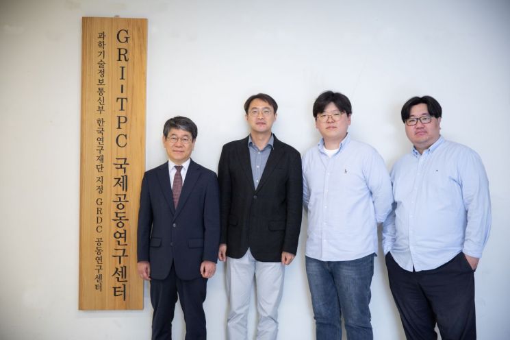 The research team is taking a group photo. (From the left: Hong Seok-ryun, Hong Young-jun, Jung Joon-seok, Cha Jang-hwan)
Typically, to manufacture semiconductors as flexible devices, semiconductors are fabricated as thin films on single-crystal wafers, then these thin films are detached from the wafers, cut into small chips, and assembled onto flexible substrates with pre-formed wiring. During the process of detaching the thin film from the wafer, work is required to break the strong chemical bonds between them. Usually, laser or chemical etching, which is costly and can degrade semiconductor performance, has been applied.
The research team stated, "As micro LEDs are attracting attention as a high value-added industry and next-generation display light source to overcome the shortcomings of OLEDs, it is significant that we have developed a technology to manufacture deformable and cuttable light sources on a large scale through a large-area current injection process."
© The Asia Business Daily(www.asiae.co.kr). All rights reserved.
![User Who Sold Erroneously Deposited Bitcoins to Repay Debt and Fund Entertainment... What Did the Supreme Court Decide in 2021? [Legal Issue Check]](https://cwcontent.asiae.co.kr/asiaresize/183/2026020910431234020_1770601391.png)


