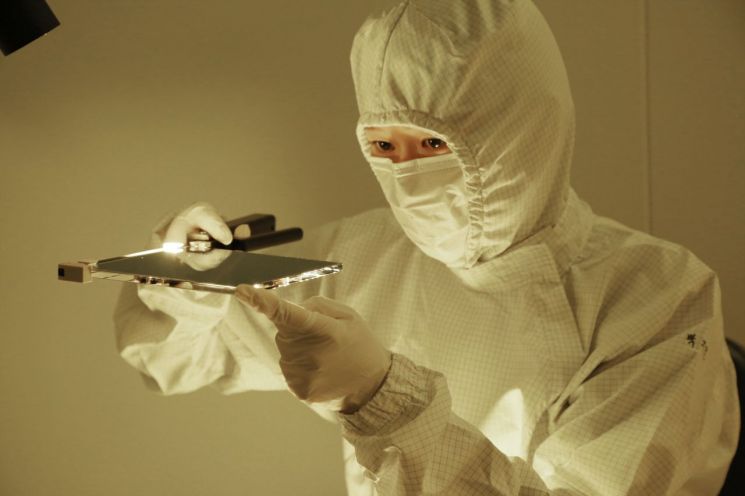
[Asia Economy Reporter Hwang Yoon-joo] SKC has embarked on the localization of high-end blank mask products, which are key materials used in the semiconductor lithography process. A blank mask is a core material used to etch electronic circuit patterns onto semiconductor wafers, and the high-end blank masks have been dependent on imports.
Recently, SKC has begun full-scale production of prototype products for customer certification at its high-end blank mask factory in Cheonan, Chungnam. SKC invested approximately 43 billion KRW and started construction of the factory in April last year, completing it in December and preparing for mass production. The goal is to commercialize as early as this year after customer certification.
The factory is located on available land within the SKC Hightech & Marketing Cheonan plant. SKC plans to develop this site into the SKC Semiconductor Materials Cluster, producing semiconductor materials. Centered on the Cheonan cluster, SKC aims to contribute to increasing the localization rate of semiconductor materials, currently about 50%.
A blank mask is the raw material for a photomask used to etch circuits onto semiconductor wafers. It is made by coating a quartz substrate with a metal film and a photoresist layer. When a circuit pattern is formed on this, it becomes a photomask. In terms of film, the blank mask is like unexposed film, and the photomask is like exposed film. When the photomask is placed on a semiconductor wafer and exposed to light, a chemical reaction occurs in the exposed areas, forming the circuit.
The blank mask market size is growing annually. Demand is increasing as semiconductor manufacturers actively expand production, and the amount used per process has increased due to finer processes. According to internal research, the global market size, which was about 800 billion KRW in 2018, is expected to grow by 7% annually to reach approximately 1.3 trillion KRW by 2025.
About 95% of this market is dominated by two global Japanese companies. Especially, the high-end market is known to be occupied by over 99%. This is due to the high entry barriers. South Korea also depends mostly on imports for high-end blank masks required for semiconductor manufacturing.
An SKC official said, "Having pursued BM innovation for several years, SKC has completed the first phase of innovation and is now advancing the second phase focused on semiconductors, mobility, eco-friendly, and display businesses. We will strive to enhance the semiconductor business and increase localization rates centered on the SKC Semiconductor Materials Cluster established in Cheonan."
© The Asia Business Daily(www.asiae.co.kr). All rights reserved.
![User Who Sold Erroneously Deposited Bitcoins to Repay Debt and Fund Entertainment... What Did the Supreme Court Decide in 2021? [Legal Issue Check]](https://cwcontent.asiae.co.kr/asiaresize/183/2026020910431234020_1770601391.png)


