Visited Samsung Advanced Institute of Technology on the 25th for inspection
"We must thoroughly prepare for the future, especially in difficult times" message
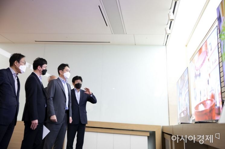
[Asia Economy reporters Changhwan Lee and Dongwoo Lee] Samsung Electronics Vice Chairman Lee Jae-yong (photo) visited the Samsung Advanced Institute of Technology to review next-generation future technology strategies and Samsung's growth engines.
This marks the sixth on-site management visit this year, delivering a continuous message to employees that despite the difficulties and challenges posed by the COVID-19 pandemic, it is essential to thoroughly prepare for the future.
According to Samsung Electronics on the 25th, Vice Chairman Lee visited the Samsung Advanced Institute of Technology located in Suwon, Gyeonggi Province, in the morning to receive a report on the status of new technology research and development (R&D) and to review next-generation future technology strategies.
Established in 1987, the Samsung Advanced Institute of Technology employs about 1,200 researchers who conduct basic research and pioneering development of core foundational technologies. Next-generation semiconductors, artificial intelligence (AI), autonomous driving, displays, and secondary batteries?Samsung Electronics' future growth drivers?are developed here.
During the meeting chaired by Vice Chairman Lee, discussions were held on pioneering technologies such as next-generation AI semiconductors and software algorithms, quantum computing technology, future security technologies, and innovative materials for semiconductors, displays, and batteries. Additionally, strategies for the Fine Dust Research Institute, established last year to address the social challenge of fine dust pollution, were reviewed.
Present at the meeting were Kim Ki-nam, Vice Chairman of Samsung Electronics' Device Solutions (DS) Division; Hwang Sung-woo, President and Head of the Samsung Advanced Institute of Technology; Kang Ho-kyu, Head of Samsung Electronics Semiconductor Research Center; and Kwak Jin-oh, Head of Samsung Display Research Center.
Vice Chairman Lee stated, "It is precisely in difficult and challenging times that we must thoroughly prepare for the future. The way we can repay the support of the people is through innovation, and when we feel we have hit a limit, we must gather strength once again to overcome the wall."
Vice Chairman Lee has been actively engaging in on-site management visits this year. Starting with a visit to the Semiconductor Research Center at Samsung Electronics' Hwaseong plant on January 2, he also conducted on-site management at the Manaus subsidiary in Brazil on the 27th, visited the Extreme Ultraviolet (EUV) line at Samsung Electronics' Hwaseong plant on the 20th of last month, the Samsung Electronics' Gumi plant on the 3rd, and the Samsung Display Asan plant on the 19th.
The visit to the Samsung Advanced Institute of Technology marks the sixth on-site management visit this year. It is analyzed that these visits aim to encourage employees facing difficulties due to COVID-19 and to prepare for a better future by turning this crisis into an opportunity.
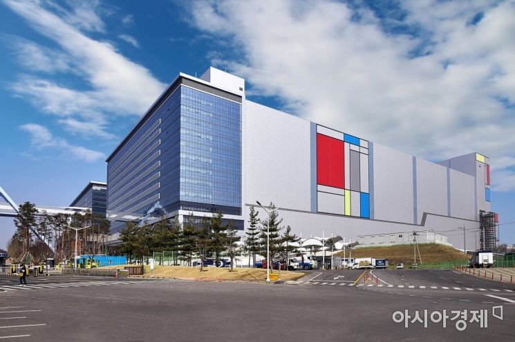
Vice Chairman Lee has shown great interest and attention to the research of 'EUV technology,' which is essential for developing high-performance, low-power semiconductors in AI, 5G mobile communications, and autonomous driving fields.
In particular, he personally visited the EUV construction site during the system semiconductor vision declaration ceremony in April last year, and in January and February this year, he visited the Hwaseong Semiconductor Research Center and the world's first EUV-dedicated production base, the V1 line, accelerating next-generation semiconductor development.
The EUV process uses an EUV wavelength light source in the photolithography process. Applying this technology reduces multi-patterning processes, improves accuracy, enhances performance and yield, and shortens product development time.
Thanks to this, Samsung Electronics' business achievements based on EUV process technology are gradually becoming visible. Samsung Electronics announced that it has established a mass production system by applying the EUV process to DRAM for the first time in the industry.
Samsung Electronics is currently developing '4th generation 10-nanometer class (1a) DRAM mass production technology' in the early 14-nanometer range using the EUV process. The 4th generation 10-nanometer class (1a) DRAM made using EUV doubles productivity per 12-inch wafer compared to the 1st generation 10-nanometer class (1x) DRAM, further strengthening business competitiveness.
Lee Jung-bae, Vice President of the DRAM Development Office at Samsung Electronics Memory Business Division, emphasized, "By applying the EUV process to DRAM mass production for the first time in the industry, we can provide more differentiated solutions to global customers ahead of others. Next year, we will continue to contribute to the sustained growth of the global IT market by pioneering next-generation products with innovative memory technologies."
© The Asia Business Daily(www.asiae.co.kr). All rights reserved.


