[Asia Economy Reporter Junho Hwang] Domestic researchers have discovered a nano-sized conductive path in boron nitride, a material widely used as an insulator because it does not conduct electricity. By forming a one-dimensional atomic-thickness electrode channel, this finding is expected to contribute to the miniaturization of semiconductor devices. On the 6th, the Multidimensional Carbon Materials Research Group at the Institute for Basic Science announced that they found a conductive channel only 1.5 nm thick?one million times thinner than a human hair?at the boundary of stacked layers of hexagonal boron nitride (hBN), a representative two-dimensional insulating material.
Insulator That Conducts Electricity
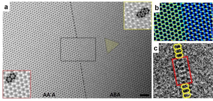
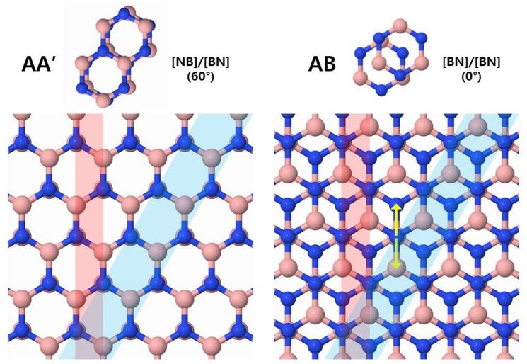 Atomic structure observed by transmission electron microscopy of the channel formed at the AA'AB stacking interface
The research team revealed the existence of the conductive channel in boron nitride using chemical vapor deposition. Boron nitride has a hexagonal shape with boron and nitrogen atoms positioned at each vertex. When boron and nitrogen atoms are exactly aligned on top of each other, the structure is called AA stacking, and when they are staggered, it is called AB stacking. The conductive path was discovered at the boundary where these two stacking structures meet.
Additionally, the team identified the precise form of this conductive path through atomic-resolution transmission electron microscopy (TEM) and image simulation analysis.
Will Transparent Devices Emerge?
 Lee Jong-hoon, Group Leader of the IBS Multidimensional Carbon Materials Research Division, and Park Hyo-joo, Research Fellow
The research team expects this discovery to have limitless applications in next-generation electronic devices such as flexible and transparent devices.
The team explained, "In electronic devices combining conductors and insulators, a passivation process is required to stabilize the surfaces of the two materials. However, the device developed by our team has an intrinsic electron pathway within the insulating hBN, so it does not require a separate passivation process."
Group leader Jonghoon Lee said, "Until now, in the field of two-dimensional electronic devices, hBN has played a supporting role that highlights the main character, graphene. Now that we have demonstrated that hBN can act both as an insulator and a conductor, the application range can be infinitely expanded to include hBN-based single-electron devices."
The research results were published on the 7th (local time) in Science Advances.
© The Asia Business Daily(www.asiae.co.kr). All rights reserved.


