[Asia Economy Reporter Junho Hwang] A domestic small and medium-sized enterprise (SME) has succeeded in achieving technological independence for core materials used in memory semiconductors. It is expected that companies, which had relied on Japanese products and were concerned about export regulations, will now be able to utilize domestically produced products.
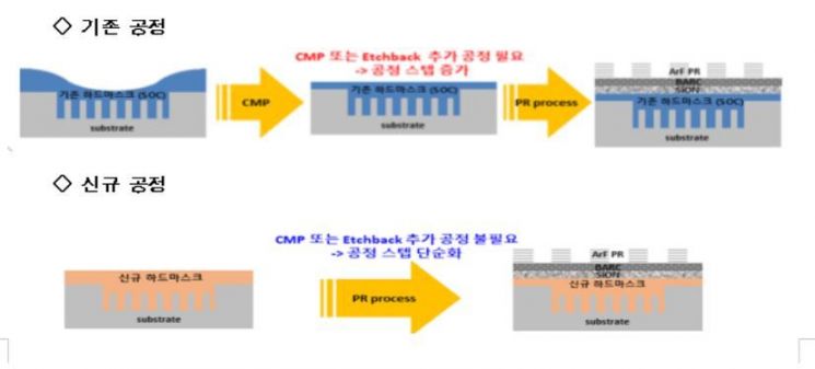
On the 12th, the Ministry of Science and ICT announced that DCT Material and the Nano Convergence Research Institute have jointly succeeded in achieving technological independence for spin-coating hard mask materials with a high aspect ratio structure used in memory semiconductors, which had been dependent on imports from Japan and other countries.
A hard mask is an auxiliary material for photomasks used to etch semiconductor microcircuits. It is an essential process material for engraving circuits on semiconductors.
DCT Material, located in Jincheon, Chungbuk, is a company producing semiconductor process materials. It had faced difficulties developing products for large corporations due to aging semiconductor material production equipment. Through collaborative research with the Nano Convergence Research Institute, they developed spin-coating hard mask materials for memory semiconductors that meet the delivery conditions of large corporations.
DCT Material’s material exhibits superior heat resistance and planarization characteristics compared to Japanese products, and also has price competitiveness. The government expects that domestic alternatives for hard mask materials used in memory semiconductors, which had depended on foreign products such as those from Japan, will become available.
A representative from DCT Material stated, "Through cooperation with the Nano Convergence Research Institute, we succeeded in developing products that surpass the world’s highest standards. If the testbed supporting SMEs is expanded in the future, we expect to accelerate technological independence in semiconductor materials."
Ko Seogon, Director of Basic and Fundamental Research Policy at the Ministry of Science and ICT, said, "We plan to actively utilize nano-infrastructure institutions such as the Nano Convergence Research Institute to support technological independence in core semiconductor materials, parts, and equipment. If the 12-inch semiconductor testbed is successfully established in the future, the competitiveness of the domestic semiconductor industry could be greatly enhanced."
© The Asia Business Daily(www.asiae.co.kr). All rights reserved.
![User Who Sold Erroneously Deposited Bitcoins to Repay Debt and Fund Entertainment... What Did the Supreme Court Decide in 2021? [Legal Issue Check]](https://cwcontent.asiae.co.kr/asiaresize/183/2026020910431234020_1770601391.png)


