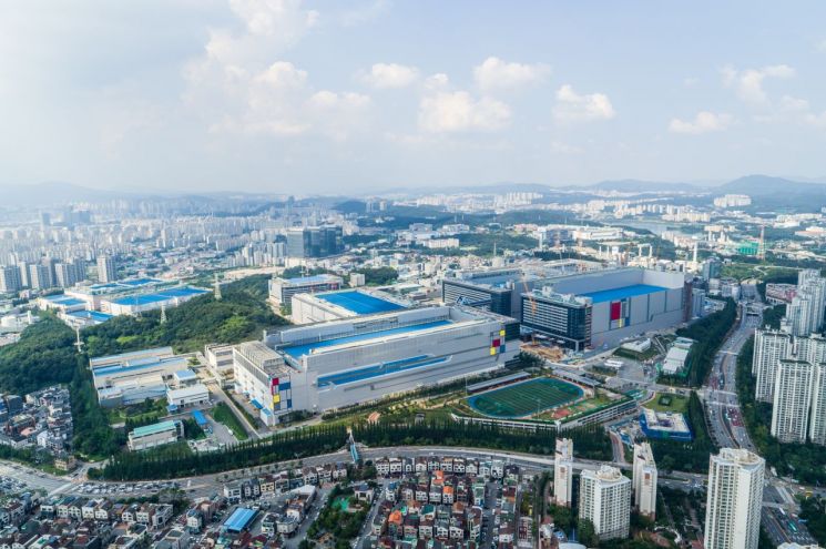
[Asia Economy Reporter Changhwan Lee] The competition between Samsung Electronics and Taiwan's TSMC in semiconductor foundry advanced process technology is expected to intensify.
According to foreign media on the 24th, TSMC plans to specifically reveal its 3-nanometer process technology at the North America Technology Symposium on April 29.
Previously, TSMC had set a goal to mass-produce 5-nanometer semiconductors by this year and 3-nanometer semiconductors by 2022, but it had not disclosed a detailed technology roadmap.
On the other hand, Samsung Electronics first unveiled its 3-nanometer process roadmap including the 'GAA (Gate-All-Around)' technology in 2018, provided design tools to customers last year, and officially announced the 'first development' this month.
3-nanometer refers to the semiconductor circuit line width. The narrower the line width, the lower the power consumption and the faster the processing speed.
Among foundry companies, only Samsung Electronics and TSMC possess advanced process technology below 7 nanometers. Samsung Electronics succeeded in development first from 7 nanometers down to 3 nanometers.
Kang Sanggu, a researcher at KDB Future Strategy Research Institute, explained in a report on the 20th, "If the 3-nanometer process is mass-produced first, the possibility of receiving orders for the latest semiconductor volumes from fabless (semiconductor design) companies increases."
© The Asia Business Daily(www.asiae.co.kr). All rights reserved.
!["The Woman Who Threw Herself into the Water Clutching a Stolen Dior Bag"...A Grotesque Success Story That Shakes the Korean Psyche [Slate]](https://cwcontent.asiae.co.kr/asiaresize/183/2026021902243444107_1771435474.jpg)


