Utilizing Copper Pillars in Semiconductor Substrates
Denser Circuit Arrangement Enables Compact Designs
Slimmer Smartphones and Improved Heat Dissipation
LG Innotek has successfully developed semiconductor substrate technology that enables smartphones to become even thinner. With this advancement, the company can now produce key components such as semiconductor substrates with the same level of performance as before, while reducing their size by up to approximately 20%.
On June 25, LG Innotek announced that it has become the first in the world to develop 'Cu-Post (copper pillar) technology' for high-value-added semiconductor substrates used in mobile devices, and has successfully applied this technology to mass-produced products.
As major smartphone manufacturers compete to make their devices slimmer, there is a rapidly growing demand for technologies that can enhance the performance of mobile semiconductor substrates while minimizing their size. In response, LG Innotek has been developing the Cu-Post technology since 2021. The core of this technology is the use of copper pillars to connect the semiconductor substrate to the mainboard. Compared to conventional methods, this allows for more circuits to be arranged on the semiconductor substrate and is also effective for dissipating heat from the semiconductor package.
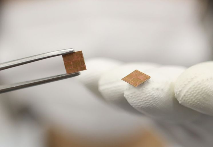 An LG Innotek employee is showcasing an RF-SiP (Radio Frequency System in Package) substrate applying Cu-Post (copper pillar) technology. LG Innotek.
A semiconductor substrate is a product that connects electronic components such as semiconductor chips, power amplifiers, and filters to the mainboard. The more densely solder balls are arranged, the more circuits can be connected. Traditionally, solder balls were attached directly to the semiconductor substrate to connect it to the mainboard, but LG Innotek's Cu-Post technology involves first erecting copper pillars and then placing smaller solder balls on top of them.
With this technology, LG Innotek has reduced the spacing between solder balls by nearly 20% compared to conventional methods. The pillar structure minimizes the area and size of each solder ball, and by using copper, which has a higher melting point, the pillar shape remains stable even during high-temperature processes, enabling even denser arrangement designs.
By applying LG Innotek's Cu-Post technology, it is possible to produce semiconductor substrates that are up to approximately 20% smaller in size while maintaining the same performance as before. Smartphone manufacturers can thus enjoy greater design flexibility and achieve slimmer device designs. In addition, this technology is optimized for high-performance smartphone functions, such as artificial intelligence (AI) computation, which require efficient processing of complex and large volumes of electrical signals. For a substrate of the same size, more solder balls can be arranged and the number of substrate circuits can be increased compared to previous methods.
 Comparison graphic of the conventional solderable attachment method and the copper post (Cu-Post) technology application method. LG Innotek.
Smartphone heat dissipation can also be improved. The copper used in the Cu-Post has a thermal conductivity more than seven times higher than that of solder, allowing heat generated in the semiconductor package to be released to the outside more quickly. This minimizes issues such as chip performance degradation or signal loss caused by heat, ensuring stable performance of mobile devices.
LG Innotek has secured around 40 related patents. The company plans to further strengthen its market leadership by applying this technology to mobile semiconductor substrates such as RF-SiP (Radio Frequency System in Package) substrates and FC-CSP (Flip Chip-Chip Scale Package) substrates.
Moon Hyuksu, CEO of LG Innotek, stated, "This technology was developed not simply for supplying components, but as a result of deep consideration to support our customers' success," adding, "We will continue to create differentiated customer value by changing the paradigm of the substrate industry with innovative products."
© The Asia Business Daily(www.asiae.co.kr). All rights reserved.


