Specializing in AI Semiconductor Packaging and Testing
Establishing a Practical Education System in Collaboration with Samsung Electronics and Others
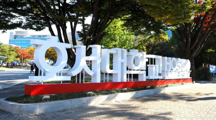
Hoseo University in South Chungcheong Province announced on June 23 that it has been selected as a final education center for the Ministry of Trade, Industry and Energy's "Semiconductor Academy" program.
Only two locations outside the Seoul metropolitan area were chosen for this project, and Hoseo University is being recognized as a key educational institution in the field of semiconductor back-end processing.
The Ministry of Trade, Industry and Energy has been implementing the "Semiconductor Academy" project since 2023, with a total investment of 23.2 billion won through 2027, to address workforce shortages in the semiconductor industry.
Hoseo University will be responsible for providing education in packaging and testing, which are essential for AI semiconductor implementation.
Located in the Chungcheong region, where the semiconductor back-end processing industry is concentrated, Hoseo University received high marks for having proactively established a specialized education system and hands-on training infrastructure in this field.
In fact, the university has set up a 680-square-meter "Semiconductor Package LAB" and secured 30 pieces of back-end processing equipment across 21 types, the same as those used by companies such as Samsung Electronics, Hana Micron, and Stats ChipPAC Korea, enabling practice-oriented training.
The curriculum was developed in collaboration with major companies in the Chungcheong region, including Samsung Electronics, Hana Micron, and SFA Semiconductor, to actively reflect industry needs. It is designed to accommodate not only semiconductor majors but also unemployed science and engineering graduates and current employees from various backgrounds.
The faculty consists of experts from leading companies such as Samsung and LG, as well as field professionals from OSAT (Outsourced Semiconductor Assembly and Test). The university plans to foster work-ready talent through field-oriented, problem-solving project-based education.
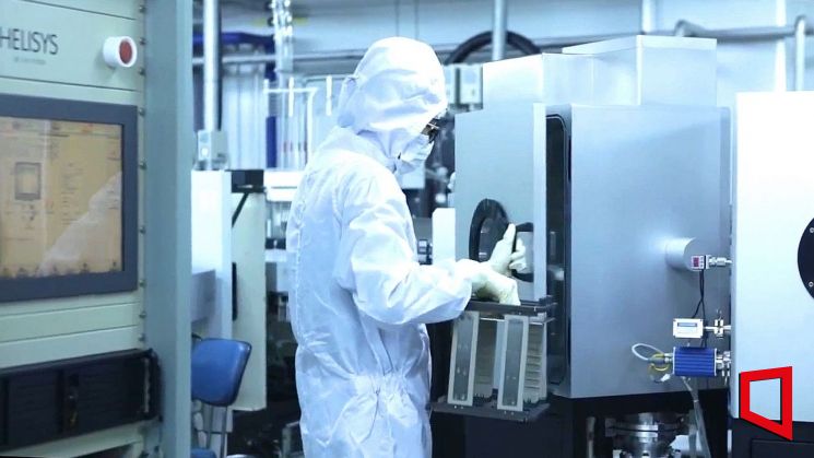 A Hoseo University student is handling semiconductor equipment in a cleanroom. Photo by Hoseo University
President Kang Ilgu stated, "Cheonan and Asan are strategic regions where the semiconductor packaging industry is concentrated," and added, "Being selected as an education center marks a significant turning point for Hoseo University to contribute to strengthening the nation's semiconductor competitiveness."
Meanwhile, Hoseo University aims to establish itself as a hub for training back-end processing specialists within the K-Semiconductor Belt through this project, and plans to create a sustainable semiconductor education ecosystem through an advanced, industry-tailored education system.
© The Asia Business Daily(www.asiae.co.kr). All rights reserved.


