Global Press Conference: No Mention of Samsung Electronics
When Asked About Samsung, the Answer Was "TSMC"
Jensen Huang: "For Packaging Technology, TSMC Is the Only Option"
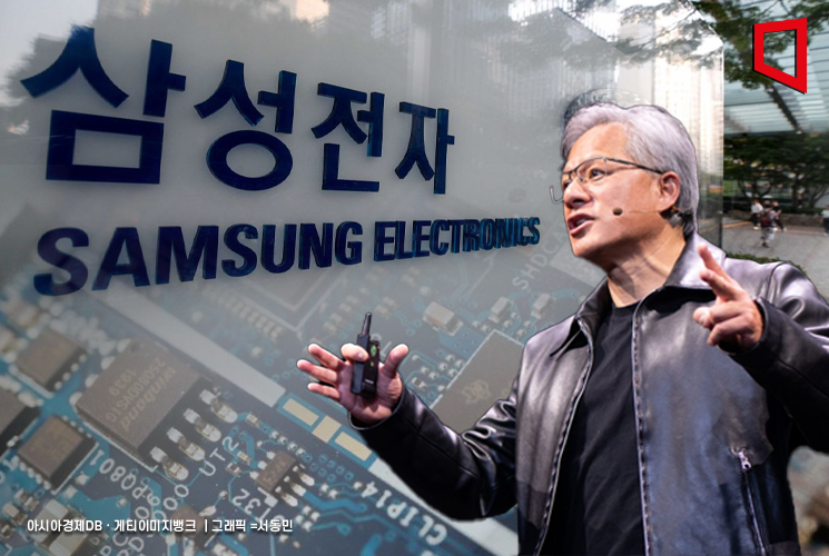
At the site of 'Computex 2025,' Asia's largest IT exhibition, not once did Jensen Huang, CEO of Nvidia, mention 'Samsung Electronics.' Even during a press conference with global media, when asked about the possibility of using Samsung's packaging technology, CEO Huang referred to the technology of TSMC, a Taiwanese foundry (semiconductor contract manufacturing) company, and dismissed the question by saying, "There is no other option."
At the GTC Taipei Global Press Conference held on the morning of the 21st at the Mandarin Oriental Hotel in Taipei, CEO Huang was asked, "How important do you think advanced packaging technology is for the development of artificial intelligence (AI)?" He responded, "Look at the size of our chips," and explained, "The way we have achieved a level beyond the limits is precisely through advanced Chip-on-Wafer-on-Substrate (CoWoS) technology."
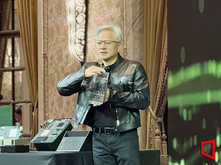 Jensen Huang, CEO of Nvidia, is answering questions at the GTC Taipei Global Press Conference held on the morning of the 21st at the Mandarin Oriental Hotel in Taipei, Taiwan. Photo by Jang Heejun
'CoWoS' is an advanced packaging method in which multiple chips are placed at very fine intervals on a wafer and then attached to a substrate. This is a proprietary technology of TSMC. The signal transmission distance between chips becomes extremely short, which dramatically increases data transfer speed and allows GPUs and high-bandwidth memory (HBM) to be positioned close together. As a result, it is considered an essential technology for maximizing the performance of AI and high-performance computing (HPC).
When asked again, "What do you think of Samsung Electronics' advanced packaging technology compared to CoWoS?" CEO Huang stated, "CoWoS is a highly advanced technology at this point in time," and emphasized, "In reality, Nvidia currently has no other option besides CoWoS." He further explained, "The reason advanced packaging technology is important in AI is because Moore's Law has effectively reached its limit." He reiterated, "The number of transistors that can be efficiently placed on a single die has plateaued, and the solution we have found is precisely this chiplet."
The latest chips are manufactured by combining multiple chips to maximize functionality. Nvidia's 'Blackwell,' which places a GPU and several HBMs on a single substrate, is an example of this.
For this reason, demand for advanced packaging technology in the semiconductor market is expected to increase even further in the future. TSMC is dominating the market for major companies' chips, such as Nvidia, Intel, and AMD, thanks to its packaging competitiveness, while Samsung Foundry has not been able to secure any significant packaging orders.
© The Asia Business Daily(www.asiae.co.kr). All rights reserved.


