Scheduled Visits to Asan Samsung Display Site
and Onyang Semiconductor Packaging Facility
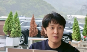
Samsung Electronics Chairman Lee Jae-yong is reportedly set to visit the Samsung Display plant in Asan, Chungnam, and the Samsung Electronics Onyang semiconductor packaging plant later this month. This move is interpreted as the start of active on-site management following his acquittal in the second trial and meetings with global artificial intelligence (AI) company leaders. In particular, it is expected that he will focus on semiconductor post-processing to boost the lagging competitiveness in semiconductor technology.
According to business circles on the 6th, Chairman Lee will visit Samsung Display and Samsung Electronics plants to assess production status and explore strategies to respond to the global market. This visit will serve as an opportunity to further strengthen on-site management across semiconductor, home appliances, and mobile divisions. A Samsung official said, "Each business site is bustling with news of Chairman Lee's visit."
![[Exclusive] Lee Jae-yong Meets Altman, Heads to Semiconductor Site Inspection](https://cphoto.asiae.co.kr/listimglink/1/2023040416341478085_1680593655.jpg)
At this point, the inspection of display and semiconductor post-processing plants is considered significant. Samsung Display, operating the Asan 1 and 2 campuses, is a key hub supplying OLED panels for global smartphones and IT devices. Recently, it has been expanding cooperation with Apple and strengthening its presence in the small-to-medium-sized market. The Onyang plant is responsible for developing next-generation packaging technology. Samsung Electronics plans to build advanced packaging facilities for high-bandwidth memory (HBM) production by 2027 using land in the Cheonan 3rd General Industrial Complex.
Chairman Lee's actions are interpreted as a strategic move to strengthen semiconductor packaging competitiveness, which has become increasingly important recently, and to respond to the changing demands of global semiconductor customers. Discussions are expected to focus on advancing post-processing technology and maximizing production efficiency to enhance competitiveness in the semiconductor business.
The resumption of Chairman Lee's on-site management coincides with the crisis Samsung Electronics currently faces in the global semiconductor market. As competitors advance in the memory semiconductor market, Samsung's sense of crisis is growing, requiring swift decision-making to close the technology gap.
Samsung Electronics is confronting multiple challenges, including a global economic downturn, instability in the semiconductor supply chain, and increasing market share of competitors. In this situation, it is assessed that rapid decision-making and strategic responses are difficult without active participation from the top management. Especially amid the semiconductor hegemony competition between the U.S. and China, proactive investment and technology development are essential for Samsung to maintain its competitiveness.
Recently, Samsung established a Management Diagnosis Office under Samsung Global Research, conducting specialized consulting to diagnose and improve management, organizational, and work processes upon requests from each affiliate. Chairman Lee's on-site visit is expected to signal the beginning of change.
In the past, Chairman Lee has created important management momentum by personally overseeing key business sites. Starting with attending the groundbreaking ceremony of the Pyeongtaek semiconductor plant in 2015, he visited the Geoje Samsung Heavy Industries shipyard to review business directions amid the shipbuilding industry crisis. In the same year, he attended the groundbreaking ceremony of Samsung Biologics Plant 3 in Songdo, emphasizing the bio business as a future growth engine. During his visit to the Giheung semiconductor research center in 2020, he highlighted the uncertainty in the global semiconductor market and stressed crisis response strategies. Last year, he visited the Giheung and Hwaseong campuses to inspect the next-generation semiconductor R&D complex and discuss technology development directions to strengthen semiconductor business competitiveness.
Changes at business sites are also expected following the visit. In the past, after Chairman Lee personally managed business sites, organizational restructuring, increased investment, and strengthening of new businesses followed. Samsung's future strategy is expected to be concretized after Chairman Lee's on-site visit. Attention will also focus on whether new business expansions such as AI, automotive electronics, and batteries will proceed.
© The Asia Business Daily(www.asiae.co.kr). All rights reserved.


