Samsung Electronics is strengthening its post-processing areas such as semiconductor packaging and testing, and is launching its first new employee recruitment for the newly established Advanced Packaging (AVP) business team this year. Lin Jun-cheng, who was known as a packaging expert at Taiwan's TSMC, the world's number one foundry (semiconductor contract manufacturing), has also been recruited as a vice president of the AVP business team. As it has become important to pack semiconductors densely within a single substrate, this move is a strategic step to actively grow the AVP business team starting this year.
Samsung Electronics' 2023 new employee recruitment announcement, which accepts applications until the 15th, includes the DS (semiconductor) division's AVP business team. The AVP business team is a newly created organization established this year. The job fields within the AVP business team are broadly divided into three areas: semiconductor process technology, packaging development, and equipment technology.
The semiconductor process technology field researches and develops foundational technologies related to fab (factory) unit processes such as photo (Photo), etching (Etch), cleaning (Clean), and chemical mechanical polishing (CMP), as well as packaging assembly processes and testing processes, to reduce defect rates and improve productivity of mass-produced advanced packaging products. It also develops production equipment that can enhance process efficiency and manages technical support and review bodies to improve equipment completeness. The packaging development field mainly focuses on circuit design for customer-tailored advanced packaging. It is also responsible for product, structure, and material development and simulation of advanced packaging. Additionally, equipment technology involves maintaining, repairing, modifying, and improving equipment to realize a semiconductor manufacturing environment for producing the highest quality advanced packaging products.
Samsung Electronics established the AVP business team because next-generation packaging technology has become important, especially in the high-performance computer market. Semiconductor packaging processes refer to manufacturing semiconductors into forms suitable for electronic devices. It is an essential step that creates pathways for electrical signals and processes the exterior to commercialize the product. High-performance and low-power semiconductor packaging technologies are required in various fields such as artificial intelligence (AI), 5G, and automotive electronics.
In the past, semiconductor companies focused intensely on ultra-miniaturization competition, but now that semiconductor miniaturization technology has reached its limits, it has become important to efficiently and densely pack many semiconductors on a single substrate. Enhancing post-processing capabilities to maximize semiconductor performance has become crucial. Market research firm Gartner forecasted that the semiconductor post-processing market, which was $48.8 billion (approximately 63.62 trillion KRW) in 2020, will grow to $64.9 billion (approximately 84.6 trillion KRW) by 2025. Samsung Electronics Chairman Lee Jae-yong also visited the Cheonan and Onyang campuses, where semiconductor packaging lines are operating, last month to check packaging competitiveness and research and development (R&D) capabilities.
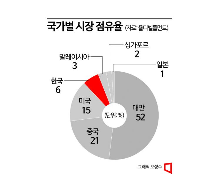
Samsung Electronics formed the AVP organization as a task force (TF) under President Kyung Kye-hyun in June last year, and this year, by establishing the AVP business team, it is focusing on creating a complete organization. Vice President Lin, who worked as a semiconductor packaging expert at TSMC from 1999 to 2017, is responsible for advancing related technologies in the newly established team. He is in charge of the AVP development office within the AVP business team. Taiwan holds a 52% share of the global semiconductor market's post-processing sector, which is higher than Korea's 6%. Taiwan's technology is more than 10 years ahead of Korea's. Prior to recruiting Vice President Lin, Samsung Electronics also appointed Kim Woo-pyung, formerly of Apple, as the head of the U.S. Packaging Solutions Center to strengthen packaging technology capabilities.
© The Asia Business Daily(www.asiae.co.kr). All rights reserved.


