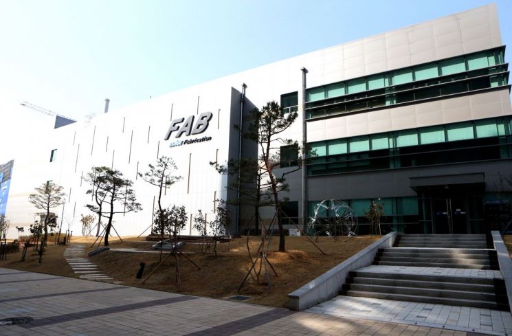
[Asia Economy Reporter Hwang Junho] The Central Equipment Center at Daegu Gyeongbuk Institute of Science and Technology will open a semiconductor process device cleanroom capable of fabricating complementary metal-oxide-semiconductor (CMOS) devices starting from the 12th. Schools and research institutes that lack related facilities will be able to utilize this facility for various research activities, such as the development of next-generation semiconductor device technologies based on CMOS in the future.
The Central Equipment Center has additionally established a 0.5μm-class CMOS standard process line aimed at enhancing intelligent semiconductor research capabilities and creating value through semiconductor manufacturing process utilization. This enables integrated device fabrication rather than unit process-level production. It also supports semiconductor-related research such as testing research devices that must operate at the CMOS level, providing platforms for developing new semiconductor devices and materials based on CMOS, supplying CMOS unit wafers, and supporting CMOS-based educational services. The center has also built a research platform capable of supporting semiconductor processing and nanoanalysis. Through this, integrated services such as material and device verification, analysis, and demonstration can be utilized. Additionally, the center is equipped with a 6-inch-based semiconductor process device cleanroom and various research equipment.
Center Director Lee Bong-ho said, "With the global foundry market growing and the increasing need for research and development among domestic industry, academia, and research institutes, we proceeded with the expansion of the CMOS standard process line. We believe this will greatly assist many researchers, including local companies, in their research on next-generation semiconductors."
© The Asia Business Daily(www.asiae.co.kr). All rights reserved.


